
More powerful mobile devices, larger televisions, autonomous and electric vehicles, wearables, virtual reality, and the Internet of Things (IoT)—these technologies drive innovation and efficiencies in the electronics industry and in semiconductors themselves. Ceramics serve a crucial role in enabling these developments, whether in the manufacturing, use, or application of advanced semiconductors.
While ceramic technologies do not always serve glamorous roles, they provide necessary thermal, mechanical, electrical, and environmental stability to this industry. Detailing all of the ways in which ceramics contribute to modern semiconductors is beyond the scope of any article, but there are many examples where ceramics enable essential functionalities to the materials themselves, the manufacturing process, and their application in technology.
The remarkable variety of possible ceramic compositions leads to a wide spectrum of properties useful to the semiconductor industry (Table 1). Semiconductor manufacturers employ ceramics for their mechanical and environmental stability in highly corrosive environments. Ceramics have been adopted in packaging, where hermeticity, thermal conductivity, and mechanical integrity are paramount. And in communications and sensing, ceramic dielectrics support high rates of data transmission and monitoring.

Semiconductor manufacturing
The global semiconductor market is estimated to have exceeded $410 billion in 2017, with a projected annual growth rate of more than 7% in 2018.1 In particular, solid-state memory [dynamic random access memory (DRAM) and 3-D NAND flash memory] and displays [liquid crystal display (LCD) and organic light-emitting diode (OLED)] are driving explosive demands for technologies and equipment to support larger, thinner, and better televisions (4K or 8K resolution) and cell phones and computers that can store more photos and videos. Other technologies expected to contribute to this growth include virtual and augmented reality, artificial intelligence, IoT, and autonomous vehicles.
To support these applications and the increasing number of new wafer fabs that have been announced, manufacturers of wafer fabrication equipment (WFE) face unprecedented demand for tools and components for those tools. Wafer fabrication involves various manufacturing operations, including etching, deposition, lithography, ion implantation, inspection, and polishing. Often, these processes are conducted under high vacuum and in the presence of corrosive chemicals. In addition, high temperatures and high voltages may be involved.
As such, wafer fabrication requires corrosion-resistant materials, such as stainless steel, anodized aluminum, high-temperature polymers (polyimides), and ceramics. The market for ceramics used in WFE is estimated at around $350 million, with an additional $60 million associated with LCDs. This represents a growth of approximately 50% over the past year alone—ceramic manufacturers are scrambling to meet this demand.
There are a variety of ceramic components essential in wafer fabrication processes, including wafer polishing substrates, chucks and carriers, heaters, plasma-resistant parts, nozzles, windows, and feedthrough insulators. Perhaps the most obvious use of ceramics in high-vacuum equipment is the occasionally decorative design of these electrical feedthrough insulators.
As an example, Figure 1 shows a flange-mounted evaporation source. The feedthroughs shown include mechanical manipulators in addition to high-voltage (3–10 kV) and high-current insulators. These electrical feedthroughs are manufactured using pressed Al2O3 ceramic, brazed to a FeNiCo receptacle or flange. Migration from 200-mm to 300-mm semiconductor wafer fabs creates a need for correspondingly larger heaters, carriers, and chucks. Fabrication of such parts with exacting tolerances represents a manufacturing and machining challenge.
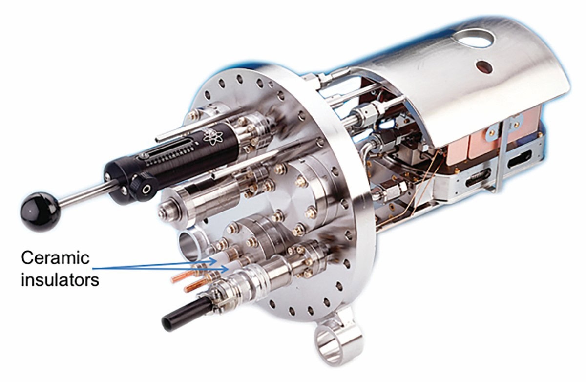
Figure 1. Ceramic–metal (high voltage, high current, and electromagnet sweep) feedthroughs are evident in this image of a vacuum evaporation source, courtesy of MDC Vacuum Products. Credit: MDC Vacuum Products
Whereas Al2O3 is a standard material, some applications require other materials. For example, efficient heat removal in plasma chemical vapor deposition (PCVD) processes is dependent on thermal dissipation through the wafer carrier. Whereas both Al2O3 and AlN exhibit the necessary high dielectric constant and good plasma resistance for PCVD, the inherent high thermal conductivity of AlN significantly reduces the magnitude and inhomogeneity of wafer temperature during processing.
Increasingly, processing requires high temperatures and aggressive chemical etchants and atmospheres. These highly corrosive gases and plasmas include reactive ions (Ar, O, and N), fluorides (CF4, SF6, and NF3), and chlorides (HCl, BCl3, and Cl2). Corrosion and erosion of carriers, masks, and chamber walls themselves introduce undesirable impurities into wafer chemistries. Thus, there is a need for both corrosion resistance and high purity.
Some examples of wafer handling chucks are shown in Figure 2. In processing, wafers are held in place by vacuum or by electrostatic forces. Electrostatic chucks employ either Coulombic or Johnsen-Rahbek forces, induced by electrodes embedded in the ceramics. Vacuum chucks are less favored as the wafer may be deformed during processing. In addition, carriers may be required to uniformly heat substrates (±1–2°C) across the full footprint of the wafer. AlN is well suited for this application, although a common requirement that the substrate be of high purity precludes the use of rare-earth oxides and other sintering aids that would increase thermal conductivity from about 70 W/m∙°K to at least 170 W/m∙°K.
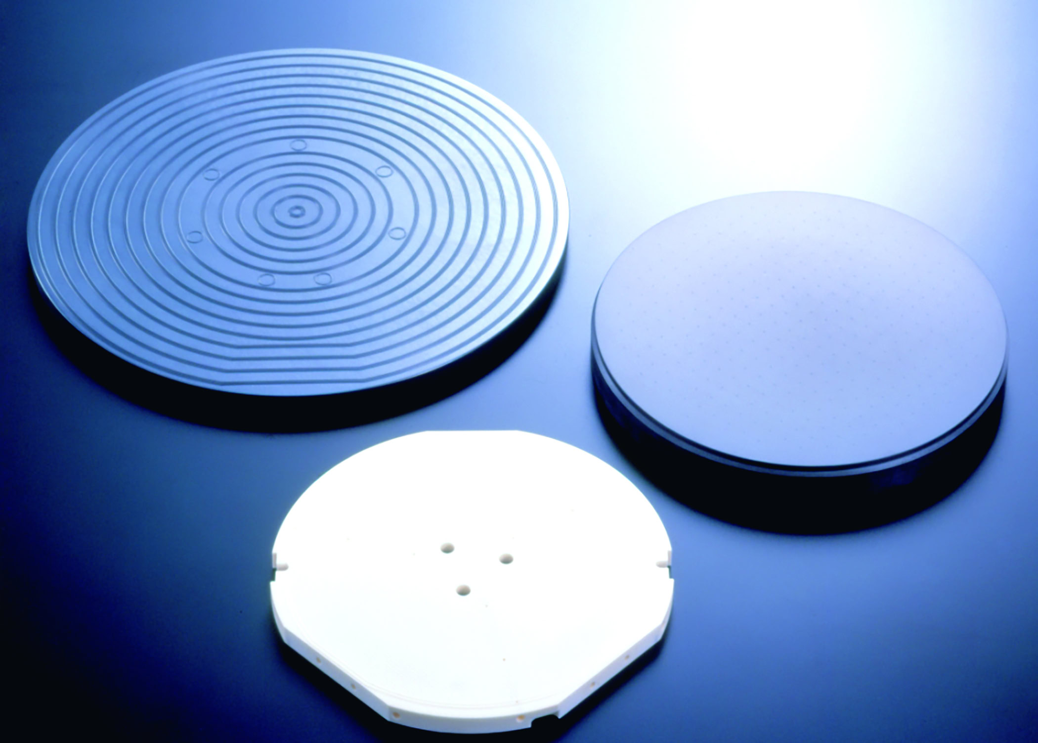
Figure 2. Ceramic vacuum and electrostatic chucks are used to secure semiconductor wafers during processing. High-purity ceramic heaters are used in corrosive environments (e.g., ion implantation, etching) where temperature uniformity is critical. These products are commonly manufactured from SiO2, SiC, Al2O3, and AlN. Credit: Kyocera International Inc.
Semiconductor packaging
Because the number of ceramics in mobile phones, televisions, Wi-Fi routers, automobiles, and beyond can be quite substantial, we focus here on a few novel applications.
Critical protection in medical devices
The use of ceramics in medical applications extends beyond bones and teeth. Although dental implants and artificial joints are important, especially for those in need of replacements, incorporation of electronics into implantable devices offers additional functionality in patient monitoring and therapy.
Cardiac pacemakers were perhaps the first example of an implanted electronic device, with widespread introduction in humans in 1960. Early pacemakers were large and prone to leakage and failure, as they were not hermetically sealed. Eventually, welded titanium enclosures and high reliability feedthroughs replaced plastic-encapsulated electronics. As shown in Figure 3, implantable devices include batteries, control devices, and circuit boards that, to function reliably for as long as 20 years, must be effectively isolated from body fluids or other potential sources of failure.
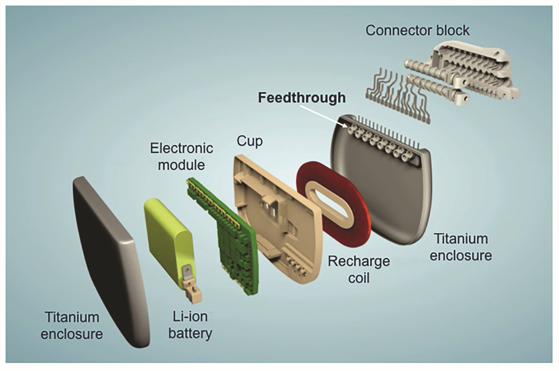
Figure 3. Exploded view of a hermetic neurostimulation device, courtesy of Medtronic. Credit: Medtronic
Ceramics and glasses play an important role in assuring this reliability, serving as insulators in feedthroughs for these devices. Traditional feedthroughs, such as those shown in Figure 4, are constructed from metal pins (Pt, Pt-Ir, Nb) sealed (Au brazing) into an alumina eyelet or embedded in a glass dielectric. This assembly is, in turn, brazed into a titanium ferrule.
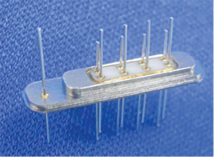
Figure 4. Standard 9-pin feedthrough, reflecting Pt-Ir pins brazed into an Al2O3 ceramic, which is subsequently brazed into a Ti ferrule. Credit: Kyocera International Inc.
As the functionality of devices increases, the number of feedthrough pins also increases. Eventually, it is no longer pragmatic or economical to braze a large number of pins into a device that, ideally, is becoming smaller and more compact. For instance, retinal implants may require as many as 100 feedthrough connections.
To address this, manufacturers have introduced a cofired technology involving use of platinum paste rather than a metal pin and multilayer Al2O3 rather than pressed or machined ceramic monoliths. Use of multilayer technology enables concentration of many leads into a much smaller volume. Figure 5 shows a crosssection of a cofired feedthrough where filled vias function in place of metal pins.
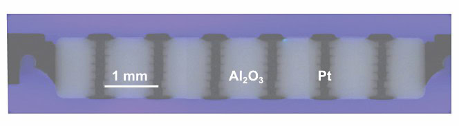
Figure 5. Optical crosssection showing a cofired, 6-terminal feedthrough. The “pins” are Pt-filled vias cofired into a multilayer Al2O3 ceramic, which has been brazed into a Ti ferrule. Credit: Kyocera International Inc.
Multilayer technology offers the opportunity to include additional functionality (antennas, power dividers, etc.) within a structure. Whereas brazed (legacy) feedthroughs are among the most reliable components in an implanted cardiac device, cofired feedthroughs have demonstrated equivalent reliability in accelerated reliability testing.2
Supporting enhanced communications
In the era of the smartphone, there are a surprising number of ceramic components within an average mobile device, including capacitors, filters, antennas, and substrates for image sensors. With the sale of mobile phones approaching nearly two billion units annually,1 the number of ceramic components in phones is at least an order of magnitude higher.
The capabilities consumers demand would be impossible without development of wireless technologies to support enhanced data rates and extended geographic coverage. More data, more users, more phones, and more remote locations mandate more capabilities in cellular infrastructure. Cell towers that dot the global landscape are high-power broadcast terminals, housing large numbers of RF amplifiers. To satisfy the expectations of consumers, service providers have mandated increased power, efficiency, linearity, and gain in power amplifier (PA) technology—and at a lower cost.
At the end of the 1990s, bipolar silicon began to be supplanted by silicon laterally diffused metal oxide semiconductor (LDMOS) PAs. Both technologies require dissipation of a substantial amount of heat. For example, high-power LDMOS PAs may transmit up to 200 W and dissipate in excess of 300 W. Bipolar devices are mounted on a ceramic insulator, typically AlN or BeO. LDMOS devices, on the other hand, are placed directly on the source electrode—an electrically conductive heat sink. To operate reliably, packaging associated with these devices must remove heat such that the maximum operating junction temperature within the semiconductors is less than 200°C.
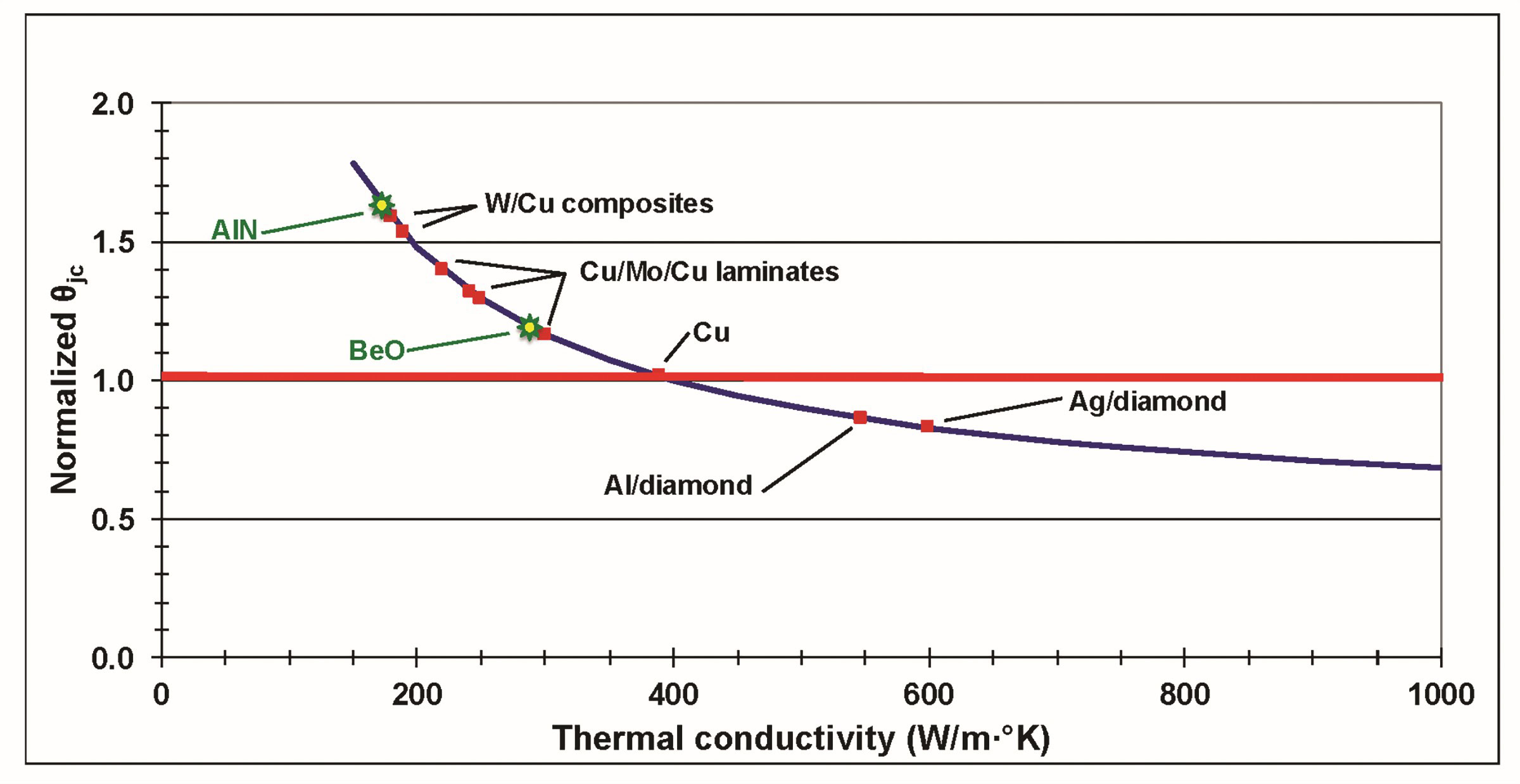
Figure 6. Thermal performance of an LDMOS-style package, as reflected in thermal resistance (θjc) normalized to a copper heat sink (thermal conductivity = 400 W/m∙°K). Note that an Al2O3 heat sink results in a normalized value of 7–12.2 Credit: Kyocera International Inc.
Figure 6 displays the efficiency of various heat sink materials. BeO is a superior insulator/heat sink for PA packaging. Unfortunately, BeO suffers from its reputation as a toxic substance and, just as importantly, is a more costly solution. AlN, on the other hand, is a slightly inferior heat sink material for high-power devices. As such, the typical LMDOS package (Figure 7) employs a relatively inexpensive composite metal heat sink. An Al2O3 “window frame” is required to electrically isolate leads from the base, which is typically under high mechanical (bolt-down) and thermal stresses.
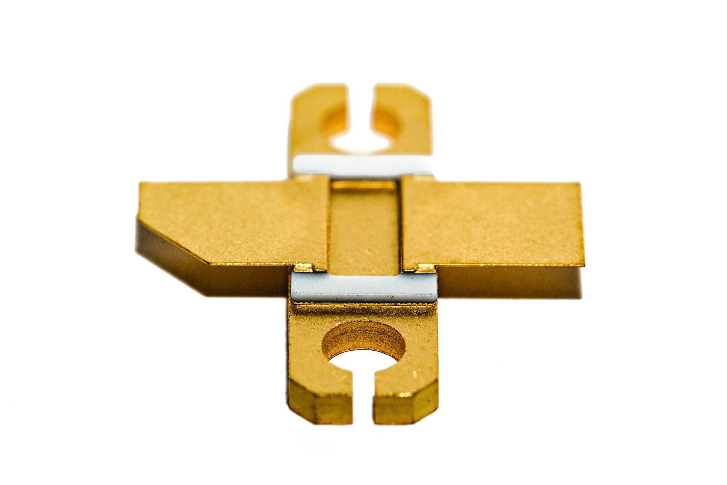
Figure 7. LDMOS package. The silicon die mounts directly onto a composite metal (Cu/CuMo/Cu) flange. An Al2O3 “window frame” insulates FeNiCo leads from the flange. Credit: Kyocera International Inc.
Data are transmitted through various media, including free space, copper wire, and optical fiber. Packaging associated with optical data transmission is ideally suited to ceramics, as repairs of optical transmission infrastructure (underground or undersea) are expensive if not impractical. Electro-optical (E/O) packaging typically requires hermeticity, rigidity (high elastic modulus), and thermal dissipation, with well-defined optical properties of transparency or opacity.
Thus, growth in mobile data in the developing world has also resulted in increased demand for E/O products. The laser diode package displayed in Figure 8 provides a good illustration of these requirements. The body of the package is metal with opaque, 90% Al2O3 feedthroughs on either side. One set of these feedthroughs includes a high-speed (5 Gbps/15 GHz) coplanar waveguide input/output (I/O).
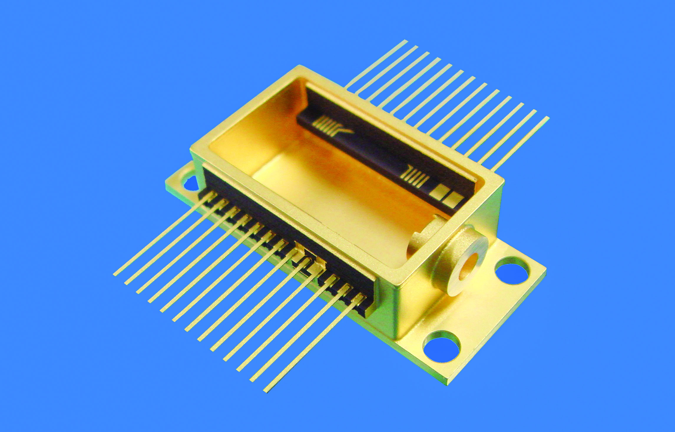
Figure 8. An electro-optical “butterfly” package including optical fiber and 15 GHz RF input/output. Credit: Kyocera International Inc.
In RF or high-speed digital applications, mechanical and thermal performance may take a backseat to electrical properties (e.g., dielectric constant, loss) of these materials. The two most significant loss mechanisms are conductor and dielectric loss. Conductor loss favors use of low-resistivity conductor metals (Ag, Cu, Au), such as those employed with low-temperature cofired ceramics (LTCC). In printed wiring board (PWB) applications, copper is the dominant metal, with a conductivity (6.0 × 10⁻⁷ S/m) only about 5% less than that of silver (6.3 × 10⁻⁷ S/m). High-temperature cofired ceramics (HTCC) typically use a refractory metal such as tungsten (1.8 × 10⁻⁷ S/m), which is then plated with nickel and gold (4.1 × 10⁻⁷ S/m).
LTCC ceramics are often promoted as low-cost alternatives to HTCC. LTCC materials are typically sintered at temperatures of around 800–900°C, allowing use of less costly furnace materials than required with HTCC (firing temperatures of 1,600–1,900°C). This cost advantage can be very dependent on the conductor metals. At roughly $1,000/Troy ounce (toz) and $1,300/toz, respectively, platinum and gold conductors can significantly add to the cost of a multilayer module.
For example, Figure 9 compares the relative costs of an LTCC and HTCC RF module. In this case, the sample package is a multicavity module measuring approximately 4 × 2.5 × 0.5 cm, with heat sinks and an RF connector block. This particular module includes a significant amount of buried conductors and ground vias for RF isolation. As such, paste costs in the LTCC module account for a whopping 56% of the total cost, dominated by the commodity price of gold powders used in the conductor paste. In contrast, the HTCC module utilizes tungsten conductors, and thus the paste represents only 5% of the cost. Overall, this LTCC module, in high volume, costs more than twice as much as a comparable HTCC module.
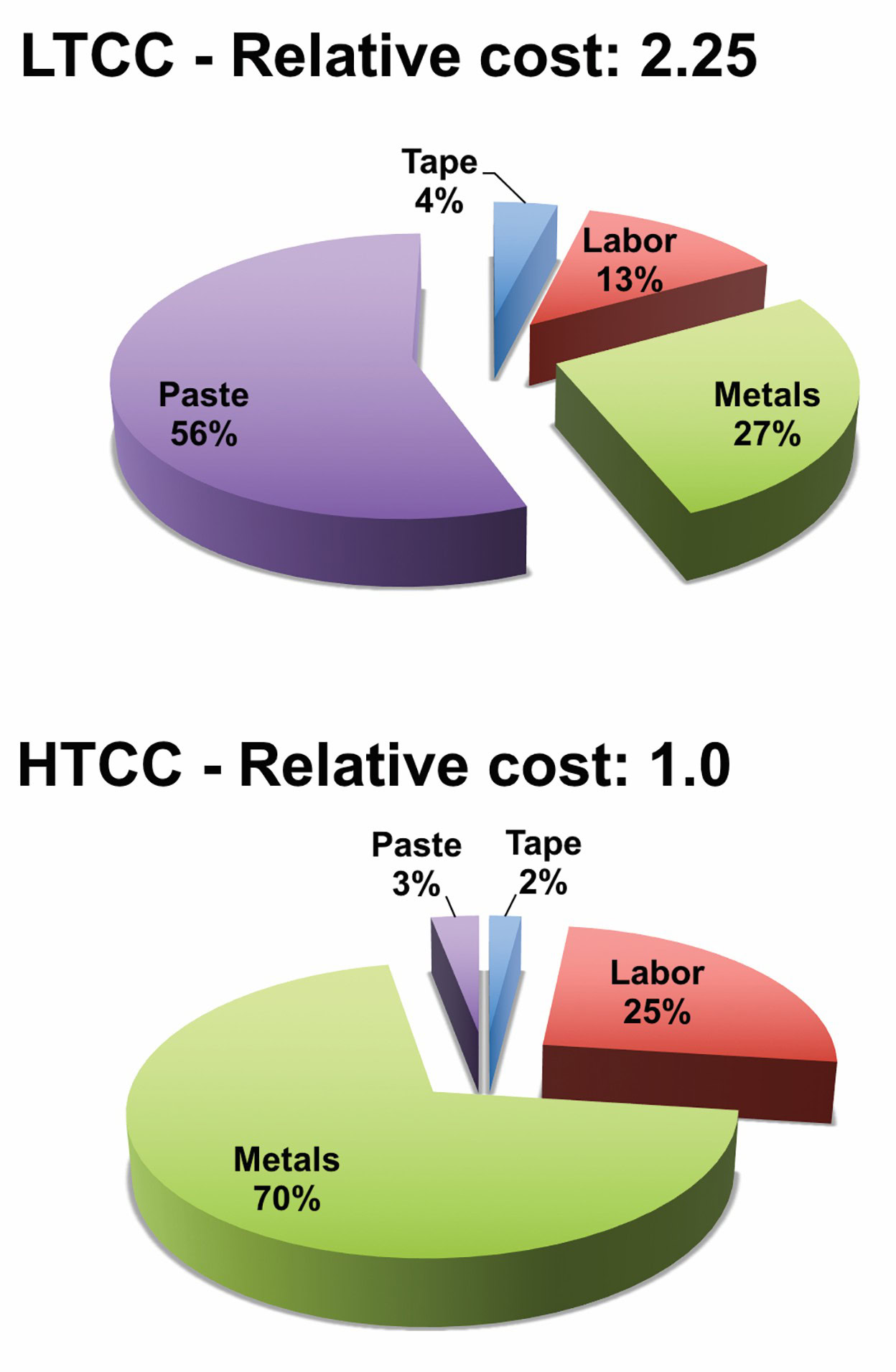
Figure 9. Comparative costs of the same RF module manufactured in LTCC (commercial tape with gold conductors) and HTCC (Al2O3 with tungsten conductors). Metal costs include heat sinks, seal rings, braze preforms, leads, and connectors. Credit: Kyocera International Inc.
The second source of loss in high-frequency packaging is dielectric loss, influenced by dielectric constant and loss tangent. The magnitude of these attributes, in addition to their variability within a material, can be critical. For example, embedded filters, important in communications and radar applications, are susceptible to small changes in dielectric constant. Fundamentally, dielectric properties can be subtly or significantly impacted by variability in ceramic density, phase chemistry, phase distribution, and impurities, among other factors. This variability can be linked to inconsistencies in chemistry, processing, and firing.
Figure 10 displays dielectric constant (Dk) distribution in various commercial HTCC and LTCC systems, taken from different raw material and firing lots. The two LTCC materials with the lowest Dk (5.9 and 7.1) also exhibit the broadest distribution. In fact, each LTCC composition with noble metal conductors features resistor, solder mask, and conductor pastes that may be printed and refired. This refiring, while offering greater flexibility in design, may alter the phase distribution within the ceramic, resulting in the type of variability observed in Figure 10.
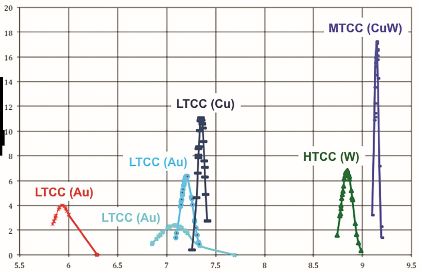
Figure 10. Distribution of dielectric constant at 10 GHz in multilayer ceramic materials: LTCC with copper or gold conductors, HTCC with tungsten conductors, and a medium-temperature cofired ceramic (MTCC) that employs a composite CuW conductor and is fired at ~1,300°C. Credit: Kyocera International Inc.
Protecting satellite electronics
Hermetic modules have been considered essential in satellite and other high-reliability applications. Costs associated with placing electronics in space and the impact of failures have mandated that reliability is paramount. Recent qualification of a “near hermetic” specification for space (NASA’s Class Y microcircuit designation) has challenged that paradigm. Ceramics can also offer weight savings over metal structures, although polymeric materials are lighter still.
Satellite electronics can be grouped broadly into power, sensing, analog/digital processing, and transmission/reception. The considerations associated with power handling are similar to those discussed earlier—efficient thermal dissipation with minimal electrical losses. Unlike terrestrial applications, where convective cooling is an important cooling mechanism, radiative cooling may become dominant in space. Thus, emissivity must be considered in the choice of materials.
The advent of available satellite views of almost anything, on top of imagery used in the prediction of weather, assessment of drought, status of sea ice, etc., may be attributed to the sensitivity and variety of sensors placed in orbit. Ceramic substrates play a large role in silicon image sensors. Whereas the overwhelming majority of image sensor substrates are found in cameras and mobile phones, large image sensors have long been placed on satellites used by both commercial and government agencies. Once again, reliability drives the choice of ceramic substrate, which may be exposed to a large number of thermal cycles over the mission lifetime. AlN, with a coefficient of thermal expansion close to that of silicon, has been used to support large-area substrates.
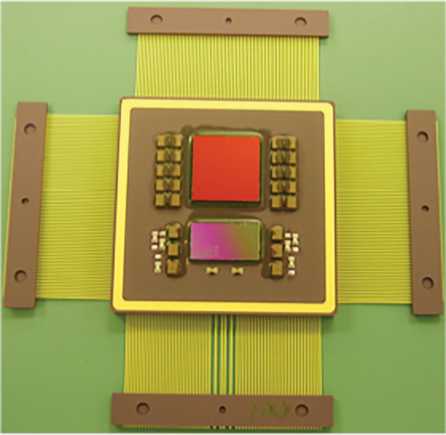
Figure 11. Satellite digital-to-analog converter (DAC). This multichip module includes Si and SiGe chips and decoupling capacitors to enhance signal integrity. The device is shown without its hermetic lid. Credit: Kyocera International Inc.
Collection of large amounts of digital images and analog data requires sophisticated image processing. Figure 11 shows a multilayer Al2O3 multichip module developed for space data processing. This particular device mandated a set of RF and digital performance metrics for both the semiconductor and HTCC substrate. An even more daunting challenge involved dimensional and reliability requirements—the hermetically sealed package was required to fit within a narrowly defined volume.
Typically, multilayer ceramics can be fired to relatively tight x–y tolerances (e.g., ±0.5% or better). However, z (thickness) tolerances are much looser (e.g., ±10%). Hardware used by the customer using the device shown in Figure 11 could not accommodate this kind of variability. Reliability testing on such a part was extensive, including evaluation of outgassing of the die attach and thermal pastes, acceleration and vibration, particle impact noise detection (PIND), and modeling to predict failures due to thermal cycling. Understandably, nothing about packaging for satellite applications is inexpensive.
Transmission between terrestrial and satellite terminals involves high-frequency signals, e.g., Ku and Ka band (10–40 GHz). Data processing, however, may use lower frequencies. Thus, there is a need for substrates and semiconductors that can efficiently process, upconvert/downconvert, and transmit/receive signals that may span 30 GHz. Figure 12 shows an example of a frequency converter package manufactured with a commercial LTCC tape system (DuPont). This multilayer part includes many RF transitions and connectors and a complex cavity structure.
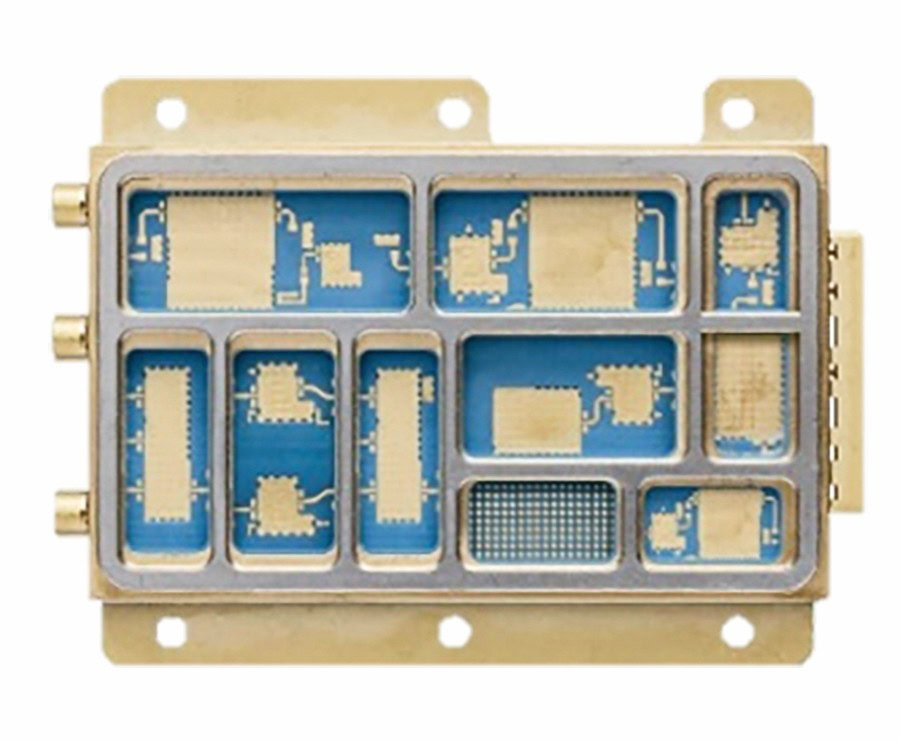
Figure 12. A satellite frequency converter package manufacured using a commercial LTCC with cofired Au conductors, RF connectors, and a complex heat sink, seal ring, and cavity structure.
Integration of functionality (amplifiers, phase shifters, attenuators, etc.) into semiconductors introduces some challenges and some flexibility in the design of packaging, where passive functions (balun, couplers, dividers, and filters) may be incorporated. LTCC is particularly well-suited for these packages because resistor and capacitor structures can be fired directly into the ceramic. Embedding load resistors proximate to dividers/couplers can increase bandwidth and decrease loss. HTCC, without cofired resistors, must rely on discrete passive components (surface mount resistors, capacitors, and inductors) placed on exposed layers. In addition, low-loss gold, silver, and copper conductors in LTCC represent a distinct advantage, with some penalty in cost, thermal performance, and strength.
High-reliability and communications antennas are increasingly migrating to a phased array architecture. Rather than utilizing a high power beam that is scanned mechanically, phased arrays provide a much more agile means of directing RF signals. A phased array can have thousands of individual radiating/receiving elements, each one individually controlled by amplifiers, phase shifters, and attenuators.
Phased arrays have been adopted for automotive radar4 and some commercial point-to-point/5G radios.5 Severe cost constraints have steered these antennas into low-cost PWB technologies. Space and high-reliability airborne antenna continue to favor hermetic ceramic solutions, however.
Like the frequency converter module shown in Figure 12, antenna modules may include cavities, connectors, and a complex array of embedded RF structures. Integration of high-performance RF connectors with low-loss interfaces is an important feature of these types of modules.
Alternatively, there are applications where much of the processing is located on a PWB substrate to minimize ceramic content. In these examples, ceramic content may be limited to tuned antenna structures, such as dielectric resonators, patches, and slots.
Phased array antenna elements are typically placed on a grid corresponding to a spacing of one-half wavelength. At 10 GHz (λ1/2 = 15 mm), this allows a relatively comfortable placement of individual or multichannel RF modules. At Ka band (30 GHz) or V band (60 GHz), however, half wavelength spacing (5 mm or 2.5 mm, respectively) mandates significant condensation of functionality and packaging.
Integrated challenges
In electronics, time is critical. Fabrication of ceramics is inherently slower than manufacturing plastics or easily machinable metals. Lead-times of 8–20 weeks are not at all uncommon—this limits the ability of customers to effectively iterate, and it penalizes mistakes.
For example, a satellite customer may wish to iterate over several potential antenna designs before committing to a specific launch design. PWB fabrication, where short lead time is a requirement and very short lead times represent a competitive advantage, can accommodate turn-around times as short as a few weeks for a complex design. This flexibility minimizes risk for customers, enabling rapid iteration and optimization when attempting to meet a specific launch window.
In the case of multilayer ceramics, green fabrication, sintering, and finishing steps typically involve expensive and time-consuming processes. Pressed ceramics require tooling, green machining, sintering, and finishing steps that also add to cost and manufacturing time.
To address these forming challenges, additive manufacturing or 3-D printing can produce complex shapes without the need for expensive or difficult tooling. However, printing of electronic devices requires printing both metallization and ceramics and, thus, also involves matching expansion and sintering rates. Whereas additive manufacturing offers tremendous flexibility for prototype or small volume applications, it has yet to be adopted in volume production.
Capsule summary
Integrated in the industry
Ceramics enable essential functionalities in semiconductor materials themselves—ultimately supporting development of smaller and more powerful electronics.
Match made in ceramics
Ceramics’ properties make the materials suitable for an array of applications, including particular roles in semiconductor manufacturing and packaging, such as transporting wafers, protecting medical devices, supporting enhanced communications, and protecting satellite electronics.
Adding future potential
Despite ceramics’ useful properties, low-cost, quick-turn manufacturing represents a market-limiting challenge. Additive manufacturing offers an attractive opportunity if it can be adopted for volume production.


Related Articles

Market Insights
Engineered ceramics support the past, present, and future of aerospace ambitions
Engineered ceramics play key roles in aerospace applications, from structural components to protective coatings that can withstand the high-temperature, reactive environments. Perhaps the earliest success of ceramics in aerospace applications was the use of yttria-stabilized zirconia (YSZ) as thermal barrier coatings (TBCs) on nickel-based superalloys for turbine engine applications. These…

Market Insights
Aerospace ceramics: Global markets to 2029
The global market for aerospace ceramics was valued at $5.3 billion in 2023 and is expected to grow at a compound annual growth rate (CAGR) of 8.0% to reach $8.2 billion by the end of 2029. According to the International Energy Agency, the aviation industry was responsible for 2.5% of…

Market Insights
Innovations in access and technology secure clean water around the world
Food, water, and shelter—the basic necessities of life—are scarce for millions of people around the world. Yet even when these resources are technically obtainable, they may not be available in a format that supports healthy living. Approximately 115 million people worldwide depend on untreated surface water for their daily needs,…