
Defects have a public relations problem—for too long, they have been regarded as the “bad guys.” Defects generally have been dismissed as deleterious to properties and performance of ceramic materials and devices, and, in turn, considerable efforts have attempted to either minimize their concentration or to counterbalance their detrimental impact.
We know, however, that defects can generate value. For example, defects and impurities cause highly desirable color in gem-quality diamonds (see table below). Today, advances in synthesis, characterization, and theoretical modeling of ceramics are beginning to challenge the “bad guy” reputation of defects.
The intentional and purposeful introduction of defects, with control over type, concentration, and location, presents an opportunity to make use of “good guy” defects. In this new role, defects are a tool for tuning and enhancing properties and even enabling new functionalities. This perspective focuses on current work and future potential for this role redefinition by highlighting advances in methodologies and scientific examples where defects have been embraced and applied to improve material function.
*From E. Gaillou, G.R. Rossman, “Color in natural diamonds: The beauty of defects,” Rocks & Minerals, 89, 66–75 (2014).
Defects and their role in materials
One role for modern materials science is to provide a foundation upon which scientists and engineers in diverse fields can address the needs of current and future societal challenges through the realization of next-generation technologies. Key to such advances is not only the development of advanced materials with novel or enhanced properties and performance, but also the know-how to synthesize and process such materials in a deterministic manner so that their properties can be effectively and efficiently utilized.
Materials science was founded upon the concept that structure, processing, properties, and, ultimately, performance of materials are intimately interconnected. And, as the field has evolved, materials scientists and engineers have increasingly realized that even our best efforts to control these tenets can be remarkably hampered if we do not account for and address the role of material imperfections. In all fields of materials science, the importance of defects is ever present; from critical flaws in a material that can dramatically reduce its strength to careful introduction of desired defects required for production of modern electronic materials, defects play an important role in the evolution of materials properties.
Underlying all this is the fact that defects are unavoidable. Even in the most “perfect” materials, there are always finite concentrations of various structural and compositional defects. In this spirit, the general opinion of defects is not a good one—defects are thought to be (uniformly) deleterious to material performance. In turn, immense efforts have been invested in understanding how to limit defect concentrations, identify defects and their locations, and even fix defects after the fact. Even the name itself, defect, carries a distinctly negative connotation. Defects are generally considered to be “bad guys” to avoid in the world of materials science.
But, armed with advances in our ability to synthesize, characterize, and model materials, this negative connotation stands poised to be redefined. So can defects really be “good guys” in materials science?
Today, even in ceramics, defects are viewed in a new light—a positive one—that casts them as another tool to design better materials and emergent properties. Such an idea is not new, and some fields have already embraced the power of defects to improve material performance over “ideal” materials. For example, in the semiconductor industry, “defects”—lovingly called dopants in a successful rebranding effort—underpin the modern electronic materials we all rely upon. There, years of development have gone into production of large-scale, high-purity crystals with extremely low concentrations of defects that have limited utility in their pristine state. Instead, once wiped clean of defects, engineers rely on their ability to deliberately “dope” defects back to precisely control properties such as conductivity.
Such an approach in ceramics has not yet been thoroughly embraced. This is not to say that there are not ceramists (in both research laboratories and industry) that do not understand, control, and utilize defects in some shape or form, but that this approach to deterministically use defects to improve material function and performance is not pervasive in ceramics. However, opportunities exist because, like group IV and III-V semiconductor systems, even small concentrations of defects can dramatically impact structural, chemical, electronic, dielectric, thermal, and other properties of ceramics.
Defect engineering in ceramics lags behind that in classic semiconductor systems for a number of reasons. First, compared to elemental/binary semiconductors, ceramics have many constituent elements and possess more diversified crystal structures. In turn, they can accommodate a wider variety of defects, including intrinsic (related to the constituent elements) and extrinsic (related to the impurities and/or dopants) point defects, point defect complexes and clusters, line defects, and planar and volume defects. Second, ceramics have a strong penchant for defects because of the relatively low energy barrier of formation and because they are readily formed to maintain charge neutrality (to compensate for impurities that are often present in the source materials and/or non-stoichiometry) due to the ionic nature of these systems. Finally, there has not been a need or strong driving force to accomplish the same level of control in ceramics, where properties can be robust even in the presence of large defect densities or one can simply “swamp-out” deleterious effects by introducing large numbers of different defects. Even source materials are generally many orders of magnitude less pure than semiconductor sources because there has not been the same driving force or need for exacting chemical control to date.
As a result, state-of-the-art defect and composition control is limited to ~1 atomic percent in many ceramics—far from the parts-per-billion control in semiconductors. This is exacerbated by the fact that there are few characterization methods that reliably measure these complex defect structures, and those that do exist are not (generally) widely applied within the ceramics community. Researchers have used theoretical, modeling, and computational approaches to study defects in ceramics, but they require considerable computational resources and have been limited to a few model systems where the approaches, potentials, and parameters are fairly well known.
As a result, a complete description of defect structures and prediction of their impact on materials behavior remains a challenging and time-consuming task. All told, these challenges have limited the advance of defect engineering in ceramics. Instead, the community typically either works to limit defect introduction in processing in the first place or to counteract deleterious effects through brute-force approaches, such as chemical alloying.
More recently, however, simultaneous advances in synthesis, characterization, and modeling of ceramics have enabled researchers to address and potentially overcome these challenges and consequently explore new ways to control and use defects as tools to manipulate material properties and function. Interest has surged in recent years, particularly in transition-metal oxides where there are intrinsically strong couplings between defects and the lattice, orbital, charge, and spin degrees of freedom that drive property evolution. It is this strong coupling, which can be manipulated with deliberate introduction of certain defect types at controlled concentrations and locations, that can provide new pathways to novel or enhanced properties and function.
From old to new school—Defects in ceramics today
The most familiar and traditional example of using defects for property control and enhancement in ceramics is chemical alloying. This approach has generally been used to enhance properties by counterbalancing undesirable effects of other defects. In electroceramics, for example, chemical alloying has long been used to reduce electronic leakage by compensating charges introduced to the lattice (in part) by off-stoichiometry and/or impurities. Chemical dopants also have been used directly to achieve desired responses, including aliovalent substitution of A– and B-site cations in perovskite (ABO3) materials to enhance ionic conduction.
Despite its long history, chemical alloying has been mainly driven by empirical observations and chemical intuition, and the “better” performance that is achieved is either only post-rationalized or poorly understood in many cases.
Synthesis and on-demand production of defects
In addition to conventional doping, advances in material synthesis techniques, such as molecular-beam epitaxy, now enable production of materials with low concentrations of grown-in defects and precise control over doping concentrations and locations. This has manifested in researchers doping wide band-gap oxides similar to traditional semiconductors and achieving high carrier mobilities, such as La-doped SrTiO3 (~104 cm2/Vs at 4K) and BaSnO3 (~150 cm2/Vs at 300K).
In addition to point defects, controlled introduction of planar defects, such as interfaces between two different materials or crystal structures, also can improve properties. Spurred by widespread access to reflection high-energy electron diffraction (RHEED)-assisted growth, researchers now use interfaces to induce new physics (e.g., observation of new topologies of polarization, such as polar vortices in ferroelectrics)1 and to improve material properties for critical applications (e.g., periodically introducing “defect” rock-salt layers in perovskite Srn+1TinO3n+1 materials—in essence making artificial Ruddlesden-Popper phases—to improve losses and quality factor for microwave applications) (Figure 1a).2
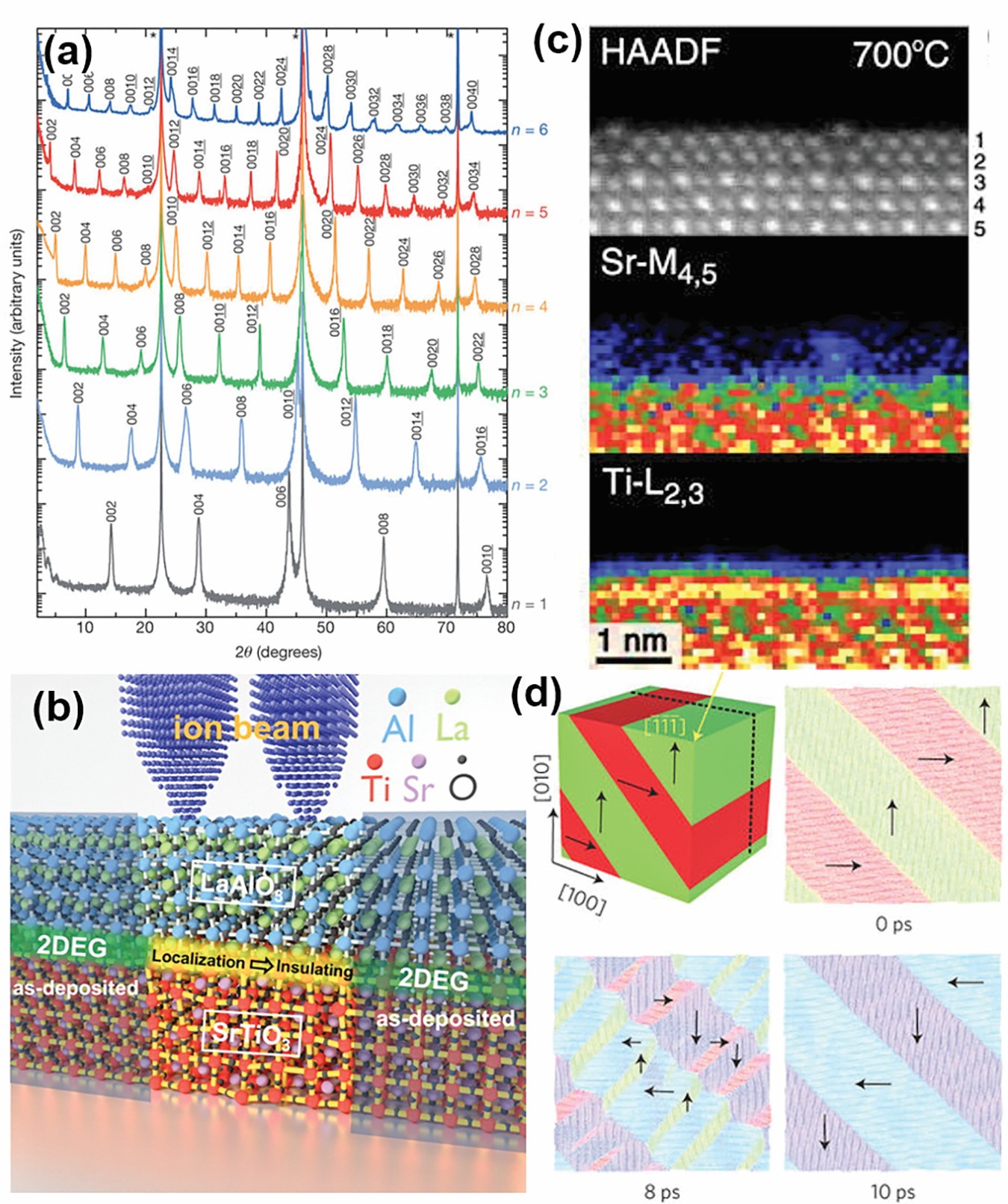
Figure 1. (a) θ–2θ X-ray diffraction scans of various molecular beam epitaxy-grown epitaxial Srn+1TinO3n+1 (n = 1–6) films, showing the deterministic ability to produce planar defects in a designer fashion. Adapted from Lee et al., 2013.2 (b) Schematic illustration of patterning of 2-D electron gas formed at the interface of two band insulators, such as LaAlO3/SrTiO3, using an energetic proton beam. Adapted from Mathew et al., 2013.5 (c) STEM-based analysis of surface reconstruction in SrTiO3 (110), including a HAADF-STEM image (top), corresponding EELS elemental maps of the same region at the Sr-M edge (middle), and Ti L-edge (bottom) at 700°C. Adapted from W. Xu et al., 2016.7 (d) MD simulation of a polydomain PbTiO3 sample with electric field applied along [111], revealing a complex domain switching process as a function of time. Adapted from R. Xu et al., 2016.8
Characterization of defects
Characterization is a foundational tenet of materials science, and progress in this regard is providing unprecedented insights into macroscopic defect responses, local/microscopic defect structures, in situ defect kinetics under stimuli, and more. Many advances have come from application of both old and new techniques developed outside ceramics. The following are a few examples of state-of-the-art defect characterization techniques now impacting ceramics.
Electrical characterization
Apart from traditional fitting of current-voltage curves for characterizing transport mechanisms in electroceramics, research has explored various characterization techniques based on macroscopic defect response under applied fields. Techniques making a resurgence or emergence include: thermally-stimulated depolarization current spectroscopy, wherein, especially for wide bang-gap materials, depolarization currents are measured while heating at a constant rate to provide information about carrier trap energies, densities, etc; deep level transient spectroscopy, which is a transient capacitance technique that monitors capacitance of a depletion region under a voltage pulse and measures carrier trap energies, densities, and captures cross-sections; and impedance spectroscopy, wherein AC impedance is measured as a function of frequency and is modeled with circuit elements to differentiate grain boundary versus bulk conduction, ionic versus electronic conduction, and other dielectric information.
Optical and magnetic characterization
Traditional optical methods, including photoluminescence and cathodoluminescence, where excited carriers release light during recombination and give information about band gap and intra-gap states, have been used for years. Other current techniques include: photoinduced current transient spectroscopy, which, especially for wide band-gap materials, uses light to excite carriers into trap states and measures current transients, thus providing information about intra-gap traps; ellipsometry, which measures changes in polarization of light as it is reflected from the material, allowing extraction of the dielectric constant along with information about surface defects; electron paramagnetic resonance, which measures the g factor of a paramagnetic ion using microwaves to move electrons between spin states split by the Zeeman effect under a magnetic field and is particularly efficient at detecting the type and orientation of defect dipoles (i.e., complexes of charged point defects).
Direct imaging and mapping
Methods today provide not only macroscopic or average probes of defects, but also local, atomic-level characterization. Advances in scanning transmission electron microscopy (STEM) together with in situ electron energy loss spectroscopy (EELS) are now a pervasive and powerful tool to directly study (and potentially produce) local defect structures and chemistry. For example, defect migration and surface reconstruction of SrTiO3 single crystals at high temperature have been directly mapped at the atomic level (Figure 1c).7 Likewise, X-ray diffraction-based techniques (typically done at a synchrotron) also are an important method to determine atomic arrangement, crystal symmetry, and chemical environment of surface and local areas of materials and can also provide insights into the presence and type of defects. Due to the extreme sensitivity to surface layers and the nondestructive nature of probing material properties, synchrotron-based X-ray diffraction has, for instance, been used to reveal the effects of defects on chemical reactions at interfaces.
Theory, modeling, and computational approaches to defects
Beyond studies of traditional metallic compounds or single/binary semiconductor materials, recent computing infrastructure developments have also led to new discoveries and understanding of functional materials with more complicated crystal structures and chemistries. From atomic- to mesoscopic-level structures, multiscale and modal techniques can predict and understand material behaviors like never before. Increased computational power and accessibility, together with better methods and more efficient approaches, today enable study of large-scale simulated cells—which resemble more realistic defect structures—at finite temperatures and allow for time-resolved studies of defect evolution under external perturbation.
Specifically in oxide materials, understanding of static/dynamic defect structures has been bolstered by application of density functional theory (DFT), Monte Carlo simulations, phase-field modeling, and molecular dynamics (MD) simulations. At the unit-cell level, DFT calculations can provide information on the stability of defect structures, kinetics, defect-induced electronic/magnetic properties, phase competition, etc. At the mesoscopic level, especially regarding defect kinetics, Monte Carlo and MD simulations building from advances in pseudopotentials are now widely used. For instance, in electrochemical applications of ceramics, understanding of ionic migration pathways and lattice interactions in materials with different structures (fluorites, perovskites, etc.) has become critical in designing next-generation solid-oxide fuel cells. Similarly, studies on gas reactions at the solid–vapor interface and kinetic incorporation of protons or ions in oxide lattices have drawn significant attention for engineering electrochemical electrode materials with high stability and efficiency. MD simulations are also used to understand dynamic lattice response of ferroelectric materials under optical excitation or electric bias (Figure 1d).8 Research is underway to explore similar approaches to understand defect dynamics.
Showing the way forward—“Good guy” defects
Armed with these techniques, researchers are beginning to reap the rewards of defect control in ceramics. Here we highlight some examples—primarily in the realm of functional electroceramics, including conducting, dielectric, ferroelectric, and magnetic properties—wherein defects are used for good today.
Functional materials and properties
As mentioned earlier, chemical alloying has long been used in ceramics to tailor properties, but such approaches have at times been guided by empirical observations and trial-and-error alone. Advances in our understanding and control of how dopants occupy the lattice and affect properties now allow us to do much better even with alloying. For example, amphoteric dopants, or “magic dopants,” choose their site according to nonstoichiometry of the lattice. These dopants are very effective in maximizing the lifetime of base-metal multilayer capacitors.9
More recent investigations have focused on controlling the type and concentration of defects beyond chemical dopants and beyond thermodynamic limits. For example, researchers have highlighted unexpected benefits of specific defect types, such as charged point defect complexes (so-called defect dipoles), due to strong coupling of electrical and elastic dipoles of such defects to the lattice and polarization. For instance, defect dipoles in BaTiO3 films enhance ferroelectric ordering by inducing additional anisotropic lattice deformation.10 Energetically preferred alignment of defect dipoles parallel to the polarization direction has also been demonstrated and used to control local polarization switching and to achieve macroscopic double-polarization switching and tri-state memory effects in BiFeO3 (Figure 2a).11
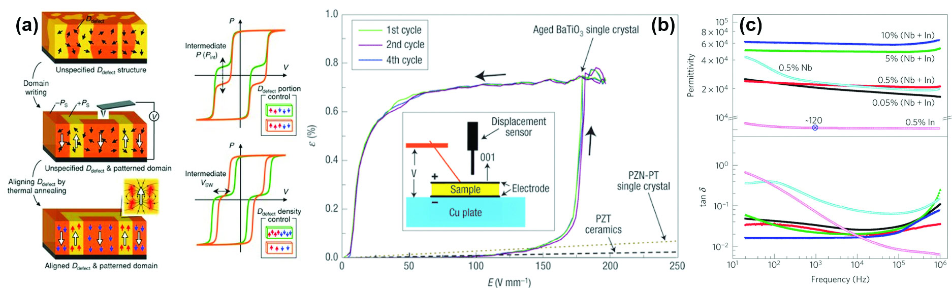
Figure 2. (a) Schematic illustration of active control of defect dipoles and associated ferroelectric switching and the resulting double-polarization switching. Adapted from Damodaran et al., 2014.11 (b) Large, recoverable electric-field-induced strain (ε) in BaTiO3 single crystals containing defect dipoles, shown compared to the piezoelectric effect of soft PZT ceramics and PZN-PT single crystals. Adapted from Lee et al., 2012.12 (c) Dielectric permittivity and loss tangent (tan δ) of Nb and In co-doped rutile TiO2 at room temperature. Corresponding properties of 0.5% Nb-only and In-only doped rutile TiO2 are also given for comparison. Adapted from Ren et al., 2004.13
Defect dipoles have also been used to enhance piezoresponse and achieve large reversible nonlinear electro-strains in BaTiO3 single crystals by providing a restoring force for reversible domain switching (Figure 2b).12 Finally, strong correlations between different defect dipoles in systems such as Nb and In co-doped TiO2 rutile can give rise to large defect–dipole clusters containing highly-localized electrons. These can, in turn, lead to colossal permittivity (Figure 2c),13 opening up promising routes to systematic development of new high-performance materials via defect engineering.
Off-stoichiometric defects also are effective in controlling and enhancing materials response if introduced in a deliberate and controlled fashion. For example, in pulsed-laser deposition of complex-oxide films, changing energetics of the growth process can be used to systematically tune defects. This growth-induced tuning of chemistry can enable fine-tuning and control of structure, dielectric response, and thermal and electrical conductivity, for example in SrTiO3, LaAlO3, NdNiO3, and BiFeO3 films.14 Off-stoichiometric defects also play a major role in ionic conduction. For example, manipulating oxygen stoichiometry has been suggested as an effective approach to manipulate the type and magnitude of ionic conduction in La2NiO4+δ. In addition, because specific cation dopants can interact with oxygen vacancies/interstitials, they have been thoroughly studied to produce better ionic materials.15
Ion-bombardment-induced defects, extensively used in semiconductors, have recently been used for property control in ceramics. This includes both intrinsic point defects (formed as a result of collision events and atomic displacements) and extrinsic point defects (formed as a result of implantation of incoming species), as well as their complexes and clusters created beyond thermodynamically defined levels. For example, recent investigations have shown the potential of bombardment-induced defects for order-of-magnitude tuning and control of resistivity, systematic tuning of ferroelectric switching dynamics, enhancement of ferroelectric and piezoelectric responses, and engineering of rewritable domain patterns in ferroelectrics (Figure 3a,b).3–5 Similar approaches have also created local structural distortions and complex nanostructured magnetic phases in La0.7Sr0.3MnO3 films (Figure 3c).6
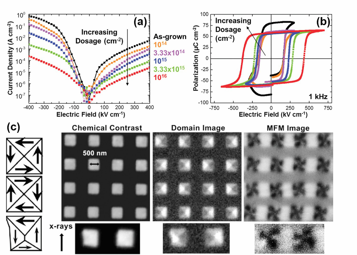
Figure 3. (a) Leakage current density as a function of DC electric field and (b) ferroelectric polarization-electric field hysteresis loops measured at 1 kHz after ion-bombardment with various He2+ dosages for BiFeO3 thin films, showing that purposeful introduction of defects can have marked impact on device properties in a positive manner. Adapted from Saremi et al., 2017.4 (c) Schematic of the domain pattern (left), together with X-ray photoemission electron microscopy-based, chemically-resolved (at the Mn-L3 edge, chemical contrast) magnetic domain structure (domain image), as well as magnetic-force microscopy-based imaging (MFM image) of 500-nm-diameter square La0.7Sr0.3MnO3 islands on SrTiO3 (001) substrates. The lower panel to each image shows effect of distortions of shape of the island. Adapted from Takamura et al., 2006.6
Further, extended defects have been used for property control and enhancement. On-demand introduction of planar defects—effectively rock-salt layers in a perovskite matrix (derived from the Ruddlesden-Popper (RP) series)—accommodates nonstoichiometry without the formation of point defects that would otherwise deleteriously dope the lattice with charge that exacerbates electrical losses.2 These same RP-type defects can also yield dramatic changes in thermal conductivity and magnetic properties.
Extended defects, along with charged point defects, also play a central role in resistive switching (i.e., electric-field-induced switching between high- and low-resistance states) for memristors. Local modulations and redistribution of defects under the switching field is considered a main mechanism for resistive switching. For instance, extended defects, such as dislocations, could act as short-circuit paths for oxygen transport and drive the material into a macroscopically detectable metallic state. Likewise, domain boundaries wherein defects such as vacancies can accumulate could also give rise to interesting transport properties.
Emergent functionalities
Purposely induced defect structures can give rise to physical properties that do not exist in a pristine version of the material. For example, oxygen vacancies are often seen as detrimental to a ferroelectric material, adversely affecting its transport and fatigue properties. In the case of SrMnO3, however, epitaxial tensile strain is accommodated by oxygen vacancies and leads to formation of a polar state in a non-d0 system.16 Similarly, oxygen vacancies have been used to engineer polar displacements in Fe in (LaFeO3)2/SrFeO3 superlattices (Figure 4a).17 In the case of magnetic materials, there are reports of oxygen-vacancy-driven ferromagnetism in TiO2, CeO2, HfO2, and a host of other oxides. Oxygen vacancies are believed to play an important role in charge redistribution as well as the exchange mechanism, though there is ongoing research and debate into the specifics of this process.
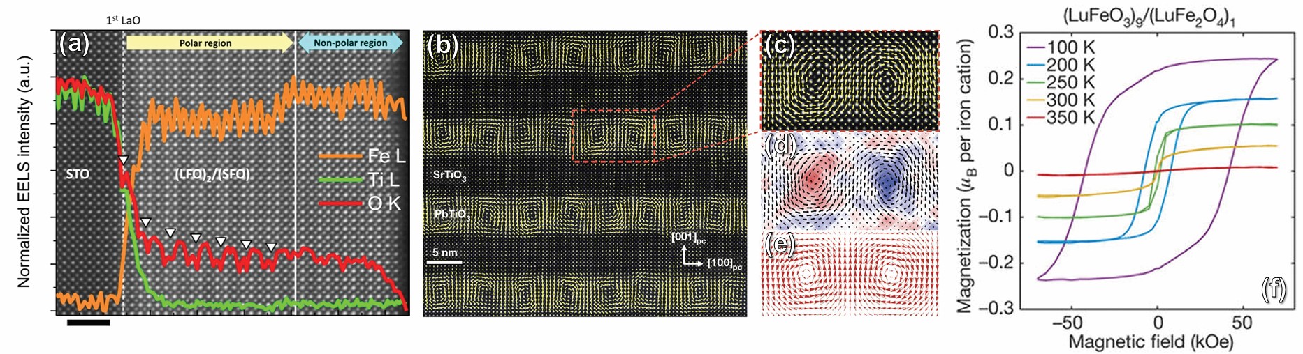
Figure 4. (a) Core-loss EELS of (LaFeO3)2/(SrFeO3) superlattice showing oxygen-vacancy ordering (denoted by arrows) in the polar region. Adapted from Mishra et al., 2014.17 (b) Atomic-displacement mapping from a STEM image of a (SrTiO3)10/(PbTiO3)10 superlattice, wherein polar vortex structures are produced. Zoomed-in view of a pair of left- and right-handed vortices in (c) atomic-displacement maps from STEM; (d) experimentally extracted polarization gradient, wherein red and blue have opposite senses or signs; and (e) phase-field simulations that recover the same structures. Adapted from Yadav et al., 2016.1 (f) Magnetization versus magnetic field loops for (LuFeO3)9/(LuFe2O4)1 superlattices at various temperatures, showing that production of interfaces between different materials can drive emergent magnetic effects. Adapted from Mundy et al., 2016.18
Surfaces and interfaces where periodicity of the crystal lattice terminates are examples of planar defects and have been the focus of much research. The most celebrated interface in recent years has been the LaAlO3/SrTiO3 system, where a 2-D electron liquid arises at the interface between two insulators. The properties of this emergent state are strongly influenced by stoichiometry and point defects.14 Superlattices also allow creation of a large number of interfaces and novel boundary conditions, allowing us to study new phenomena. Interleaving polar PbTiO3 with non-polar SrTiO3 leads to the formation of new polar states, namely improper ferroelectricity driven by octahedral rotations at short periodicities, and polar vortices with continuously rotating polarization at intermediate periodicities (Figure 4b–e).1 Superlattices of ferroelectric LuFeO3 and ferromagnetic LuFe2O4 give rise to room-temperature multiferroicity with coupling between the two-order parameters (Figure 4f).18
Functional oxides possess strong coupling among various degrees of freedom, and the resulting complexity provides a veritable playground for exploration of effects driven by competition between various energetic terms affected by defects. For example, SrTiO3 is an incipient ferroelectric material where the ferroelectric order is quenched by quantum fluctuation. However, ferroelectricity can be induced if Sr-deficient centers are produced during synthesis (Figure 5a,b).19 Similar ideas have also been applied to antiferroelectrics such as PbZrO3, where a nonpolar phase (antiferroelectric ordering) is only slightly energetically favorable compared to a polar phase (ferroelectric ordering). Under external electrical fields, phase-competition can be perturbed such that the ferroelectric phase is stabilized. Alternatively, purposely introduced point defects can also tip the energetic balance between two competing phases. In particular, antisite defects (lead atoms occupying B-site positions) can stabilize a polar (ferroelectric) ground state (Figure 5c,d).20
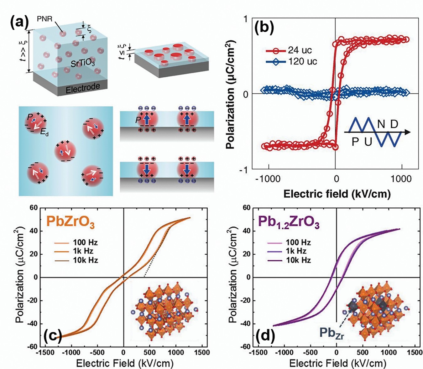
Figure 5. (a) Schematic illustration of the effect of size confinement on polar nanoregions induced by non-stoichiometry in SrTiO3. (b) Polarization hysteresis of thin (24-unit cell) and thick (120-unit cell) SrTiO3 measured using the positive-up, negative-down method. Adapted from Lee et al., 2015.19 Polarization versus electric field hysteresis loops for (c) PbZrO3 and (d) Pb1.2ZrO3 thin films show classic antiferroelectric double hysteresis loops and a ferroelectric hysteresis loop, respectively. The latter results from presence of lead-antisite defects in the lattice. Adapted from Gao et al., 2017.20
Looking to the future
As we look to the future—and in particular to the role of defects in ceramics—the near-term seems poised for dramatic advances. The work of recent decades in synthesis, characterization, and modeling are now providing unprecedented access to precisely controlled and understood materials. In turn, this opens the door for innovations. As it pertains to defects, we expect advances in several key areas.
Driven by concepts of the Materials Genome Initiative, there is strong interest in high-throughput discovery and design of next-generation materials (see, for example, PyCDT). Methodological advances that now enable the prediction and rapid assessment of complex properties are, in turn, poised to incorporate lessons of defect interactions into the design lexicon. This will enable rapid expansion of functional materials whereby designer defect structures produce new effects. At the same time, this will drive further advances in the control and study of defects. Driven by the desire to produce ever more precise structures with both atoms and a lack thereof placed in deterministic and exacting manners, experimentalists will continue to strive for ways to create, destroy, place, and move individual defects or groups of defects. Methodologies that leverage advances in aberration-corrected microscopes, scanning-probe microscopy, and coherent light sources all have the potential to provide this control. As a result, we will uncover a new era of materials engineering.
If anything has held true in science and engineering, it is that things that have sounded like science fiction in the past at some point become reality. For decades, defects have been a bad word in materials science—with entire subfields built around controlling and limiting their impact. But as our abilities to interact with materials evolve, such relationships must be reexamined.
Defects in and of themselves are not bad—they possess a set of properties and influences that, when understood and controlled, provide a depth of control and utility that could rival any other factor. Materials science has evolved from controlling materials microstructure to nanostructure to mesostructure. Perhaps the horizon that approaches us now is the era of complete control—placing atoms and using their presence and absence to create structures outside of equilibrium that have properties we have yet to imagine. In the end, defects are already showing their power for good. Further attention to them and to the power they provide scientists and engineers will only open doors for more exciting endeavors.
Acknowledgements
The authors acknowledge support from the Army Research Office under grant W911NF-14-1-0104, the U.S. Department of Energy, Office of Science, Office of Basic Energy Sciences under award DE-SC-0012375 and contract DE-AC02-05-CH11231: Materials Project program KC23MP, the National Science Foundation under grants DMR-1451219, CMMI-1434147, OISE-1545907, DMR-1608938, and DMR-1708615, and the Gordon and Betty Moore Foundation’s EPiQS Initiative, under grant GBMF5307.
Capsule summary
‘Bad guy’ reputation
Material defects generally are considered to contribute negatively to the properties and performance of ceramic materials. As such, considerable efforts have attempted to either minimize their concentration or to counterbalance their detrimental impact.
Cleaning up the act
Advances in synthesis, characterization, and theoretical modeling of ceramics are beginning to redefine the “bad guy” reputation of defects. Instead of avoiding defects, intentional and purposeful introduction of defects offers novel opportunities for materials engineering.
What’s bad is good
A new understanding is emerging that defects in and of themselves are not bad—they possess a set of properties and influences that, when understood and controlled, provide a depth of control and utility that could rival any other factor.


Related Articles

Market Insights
Engineered ceramics support the past, present, and future of aerospace ambitions
Engineered ceramics play key roles in aerospace applications, from structural components to protective coatings that can withstand the high-temperature, reactive environments. Perhaps the earliest success of ceramics in aerospace applications was the use of yttria-stabilized zirconia (YSZ) as thermal barrier coatings (TBCs) on nickel-based superalloys for turbine engine applications. These…

Market Insights
Aerospace ceramics: Global markets to 2029
The global market for aerospace ceramics was valued at $5.3 billion in 2023 and is expected to grow at a compound annual growth rate (CAGR) of 8.0% to reach $8.2 billion by the end of 2029. According to the International Energy Agency, the aviation industry was responsible for 2.5% of…

Market Insights
Innovations in access and technology secure clean water around the world
Food, water, and shelter—the basic necessities of life—are scarce for millions of people around the world. Yet even when these resources are technically obtainable, they may not be available in a format that supports healthy living. Approximately 115 million people worldwide depend on untreated surface water for their daily needs,…