
Additive manufacturing of advanced ceramics has the potential to reach a market of $4.8 billion by 2030.1 So far, additive manufacturing of ceramics has focused on niche segments such as medical applications, but there is potential for application in mass markets.
To date, the additive manufacturing methods used for advanced ceramics include stereolithography, selective laser sintering, slurry-based 3D printing, laminated object manufacturing, and direct inkjet printing.2 However, fabricating a three-dimensional ceramic body of an arbitrary shape with high density through additive manufacturing remains a challenge.2
Usually, a green body is prepared by stereolithography with photopolymerization of the binder. Large parts can be difficult to produce because of the tendency to deform and crack during binder pyrolysis. The green body then is sintered by conventional techniques.3–5
In selective laser flash sintering, poor resistance to thermal shock is an obstacle2,6 because this method creates severe temperature gradients. Higher power densities, i.e., those greater than 100 W mm–3, applied over a period of milliseconds to seconds are used.7 The outcomes remain challenging. For instance, yttria-zirconia powder could be sintered only up to 56% of its theoretical density8 and Al2O3 up to 33%.9 This method often requires further sintering in a furnace to achieve high densities.
It is possible that additive manufacturing with microflash sintering (AM-MFS) can lead to fast production of high-density parts of arbitrary shapes. Flash sintering, first discovered in 2010,10 is achieved at low furnace temperatures in very short times. The technique is demonstrated to be viable in myriad materials, including high-temperature ceramics (SiC,11,12 BC4,13 HfB214), solid oxide fuel cells (Co2MnO4,15 La0.8Sr0.2Ga0.8Mg0.2O3–δ 16), solid electrolytes for batteries (Li7La3Zr1.9Ta0.1O12,17 Li0.5La0.5TiO318), and structural ceramics (ZrO2 and Al2O3)19.
Flash sintering offers good control of process parameters because the degree of densification and the grain size are controlled by the current and the electrical field at low power.20 It has been shown to be benign in situations of constrained sintering that can cause defects in conventional sintering. In this way the sintered spots grow on the workpiece to create a component that is ready for the end user.
Initial experiments on AM-MFS
The potential of an electric field coupled with additive manufacturing was first investigated by Hagen et al. (2019).21 The authors integrated a power supply to an additive manufacturing system from nScrypt, which consisted of a slurry microdispenser and a yttrium aluminum garnet (YAG) laser. A slurry with 63 vol.% of ethanol, 25 vol.% of 8 mol% yttria-stabilized zirconia (8YSZ), and 12 vol.% of other additives was deposited on a metallic surface connected to the ground of the power supply. Then, the laser heated the deposited layers while a noncontact electrode floating over the slurry sustained an electric field of 1,000 V cm–1. Unfortunately, no enhancement in sintering was observed because of binder decomposition when heated with the laser.
Later, this same research group developed a new laser assisted method in which small regions on the surface of an 8YSZ green pellet were sintered with a laser while an electric field was sustained by electrodes in contact with that surface (Fig. 1).22 This custom-built selective laser flash sintering system reduced the necessary laser power to achieve densification.
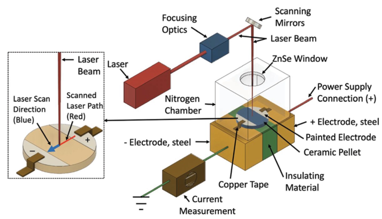
Figure 1. Schematic of selective laser flash sintering system from Hagen et al.22 Credit: Hagen et al., J Am Ceram Soc.
Electric current flowing between the electrodes was recorded with fast laser scans (spanning less than 150 ms) at low power (9.3 W). However, the results were not reproducible. A patent describing the selective laser flash sintering method was filed in 2017.23 It discusses possible configurations for a system that integrates flash sintering with additive manufacturing.
Continuous sintering via floating electrodes
In 2018, Sortino et al.24 showed that a green ceramic strip could be sintered continuously by pulling it through a pair of line electrodes, pressing it gently against the surface, and aligning them normal to the pulling direction. The electrodes were made by bending a sheet of nickel superalloy to create an edge that made “sporadic” contact with the sliding work piece (Fig. 2).24 The experiment succeeded. Key process variables were furnace temperature; field applied across the electrodes; current limit set at the power supply; and speed at which the strip, approximately 10 mm wide and 6 mm thick, was pulled through the electrodes.
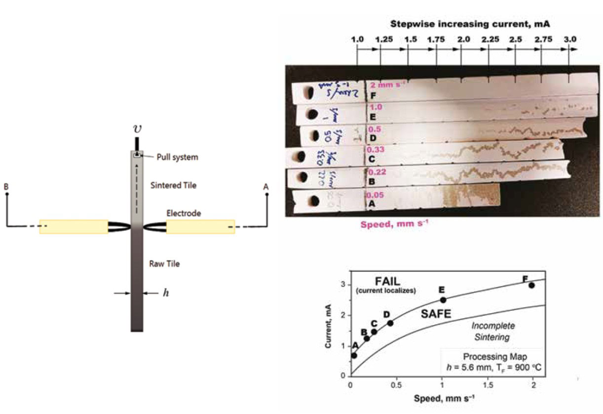
Figure 2. Experimental set-up for continuous flash experiment and processing map in terms of electric current and speed. The specimens at lower speeds show localization and defects.24 Credit: Sortino et al., J Am Ceram Soc.
The authors developed processing maps in the parameter space specified by the current density and pulling speed, and they identified three regimes. If the current was too low, then sintering was incomplete; if it was too high, it led to localization of current and poor microstructure. The safe regime lay at intermediate current densities and, rather surprisingly, at high speeds. In hindsight, they learned that uniform current densities through the workpiece could be obtained even when the contact between the electrode and the surface of the ceramic was sporadic, without too much attention being given to obtaining a good contact. Video images of the process gave clear evidence of the formation of a plasma at the interface between ceramic and electrode, which evidently was enabling uniform current flow, acting as a pseudo floating electrode.
The idea of floating electrodes that conduct current through a plasma has been pursued in different ways. For instance, Engi-Mat, a company focused on special materials applications, developed a method to join a ceramic coating into a metal substrate using a movable ionized flame.25, 26 An oxypropane flame induced electric current to the green ceramic coating, sintering it while joining it into the metallic substrate.
Saunders et al. (2016)27 used the arc plasma generated by a welder with tungsten electrodes. The authors then coupled a higher electric field through this plasma, prompting electric current to flow through a sheet of B4C. More recently, Dong et al. (2020)28 demonstrated that a cold or nonthermal plasma obtained from dielectric barrier discharge powered by radio frequency (~700 volt-ampere power source) can promote flash sintering. A disk-shaped specimen of zirconia was placed between the plasma electrode and a grounded base electrode. An AC voltage of 2 kV at 20 kHz was deployed to strike the plasma and flow current through the specimen thickness. The plasma had a large spot-size and could be applied to workpieces 5–15 mm in diameter.
Another aspect that promotes high densities is compaction and conductivity of the ceramic powders.22, 23, 27, 28 A recent patent29 describes additive manufacturing of electrically conductive materials by Joule heating. In this patent, electrically conductive powder is deposited in layers within a bed of electrically insulating powder and then compacted. The electric current flowing between the bed ground and an electrode in contact with the electrically conductive powder surface sinters its path by Joule heating, while the insulating powder in the bed serves as structural support.
Incorporating the flash sintering apparatus into existing additive manufacturing technology as proposed in Beaman et al.23 seems to be a good option to advance the technology. However, learning from recent attempts21–23 and systems,22–27, 29 it will be necessary to address three challenges to achieve the full potential of AM-MFS.
- Electrode materials and configurations. The electrodes need to be versatile for making complex shapes. They need to sustain a uniform electric current flowing through the workpiece. If a floating configuration is adopted, the plasma at the electrode–workpiece interface must stable. The applied field, which is determined by the electrode spacing should be less than 1 or 2 kV cm–1.
- Manufacturing science. The sintering rate depends on the current density flowing through the workpiece. In microflash, the uniformity of the current density in small dimensions needs to be understood. The significance of a plasma to enable uniform flow of current from the tip of the electrode into surface of the workpiece remains a fundamental issue.
- Software for process control. Flash sintering requires precise control of the voltage and current at the 10–100 millisecond time scale. Different electrical cycles can be used to optimize densification and microstructure evolution. Therefore, software is a critical aspect of AM-MFS.
Microflash experiments
We report microflash experiments in which sintering is confined to a small area on the surface of a powder bed. The influence of the electrode-configuration and the ceramic powder preparation was analyzed, the voltage and current signals were measured, and the microstructure was evaluated.
Two electrode-configurations are reported.
- Floating electrode that moves along the surface of a ceramic sheet placed on top of a copper plate that serves as the ground electrode. In this case, the electric current flows between the copper plate and the electrode, producing sintering along its path.
- A pair of electrodes placed in “casual” contact with the surface of a pressed powder bed. In this arrangement, the ceramic sintering takes place in the gap between the electrodes.
Both instances need a plasma between the tip of the electrode and the surface of the workpiece to achieve uniform current flow.
The powder-pressed sheet samples were made of 3 mol% yttria stabilized zirconia (3YSZ) powder (TZ-3Y from Tosoh, Japan) with or without the addition of 3 wt.% of silver powder (0.5–1.2 µm and 99.95% purity from Inframat Advanced Materials, USA). The powders were mixed manually using a mortar and pestle and pressed at 150 MPa into rectangular cross-sections
15 mm long, 3.5 mm wide, and 1 mm thick. Additionally, commercial 3YSZ tapes (from ESL Electro Science, USA), 0.36 mm thick and 10 mm wide (heated to burn out the binder), were used for Type I experiments; these results were similar to the powder pressed samples without silver.
The specimens were placed on the surface of a homemade heater held at 400°C. The heater assembly was mounted on a linear stage (LST 0750 from Zaber, Canada). The electric field across the samples was sustained by a 2 kV, 60 mA DC power supply (FC series from Glassman, USA). The voltage and current were measured continuously with a data acquisition device (DAQ USB 6008 from National Instruments, USA). The experiments were recorded with a CCD camera (DM51AU from The Imaging Source, USA). Linear stage, power supply, and video camera were controlled by a software developed on MATLAB. The microstructure of the specimens after flash sintering was examined in a SU3500 (Hitachi, Japan) scanning electron microscope.
Figure 3 shows a scheme of Type I experiments (contactless electrode) and their results. By keeping a distance of 150 µm between the electrode and specimen surface and applying 2,000 V, the air was ionized, generating a plasma and triggering flash sintering. The electrode could then be moved at 0.1 mm s–1 while sintering its path. It was noted that the plasma was erratic when flashing the pure 3YSZ sheet. The addition of 3 wt.% of silver to the 3YSZ helped to stabilize the plasma, reducing by two times the electric field necessary to sustain the flash. (Plasma stability is essential to move the electrode along the surface and achieve uniform current flow through the workpiece.)
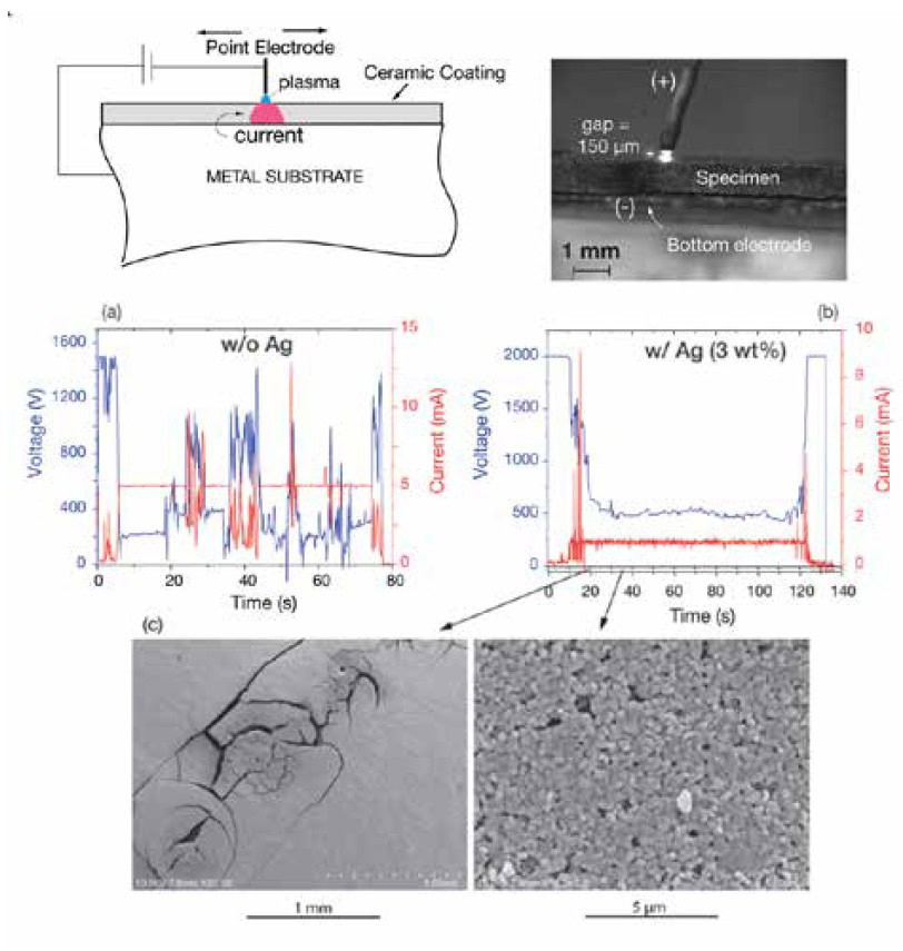
Figure 3. Type I experiments, contactless electrode. (a) The scheme. (b) Plasma formation. (c) Influence of 3 wt.% of silver on the current and voltage response. (The value of 5 wt.% in the figure on the right should have been 3 wt.%.) Credit: Ingraci Neto and Raj
Figure 4 shows Type II experiments. The pair of electrodes were placed in a “casual” contact with the sample surface; it so happened that one electrode was closer to the surface than the other. DC field with 1,500 V was applied at time (1) marked in the current profile. After the incubation time, the current rose, indicating the onset of flash (2). At this point the power supply was switched to current control to a limit of 50 mA. The light emission is from electroluminescence and plasma generation.24 The sample was kept flashing during ~30 seconds. Less than 10 seconds after the flash onset, the luminescence concentrated near the anode (3), presumably because it was separated further away from the surface than the other electrode. Flash was stable with this electrode arrangement and promoted the densification of the material between the electrodes. However, cracks developed from shrinkage strain relative to the surrounding material, as visible in Figure 4c, because of the friable nature of the powder bed. This issue should not arise in digital buildup of a dense three-dimensional body.
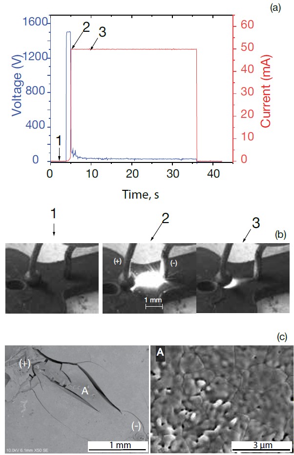
Figure 4. Type II experiments, pair of electrodes in contact with the surface of a 3YSZ specimen containing 3 wt.% silver. (a) Electric parameters. (b) Luminescence changes with time and current. (c) Micrographs of the surface after flash sintering. Credit: Ingraci Neto and Raj
Discussion and conclusions
The experiments described in Figures 3 and 4 give insights about AM-MFS.
- Doping the ceramic powders with a metal powder, at just 3 wt.% of silver, stabilized the flash parameters. The dopant also prevented the degeneration of the plasma during the movement of the electrode by reducing the electric field necessary to sustain the flash.
- A pair of electrodes could be used to sinter a small spot of material, an approach that could be used to incorporate flash sintering into additive manufacturing.
- The cracks seen in Figures 3 and 4 arise from the shrinkage of the sintered spot away from the surrounding, friable material in the powder bed. However, this shrinkage would not be an issue in AM-MFS because the dense body will be built up digitally, one small spot at a time. Because the surrounding material would be dense, cracks will not form. Also, it is demonstrated that constrained sintering becomes a nonissue in flash sintering,30 which would prevent cracking from differential shrinkage.
The role of silver addition in the experiments was to lower the field required for the onset of flash. Previous research showed that flash onset occurs at a certain level of power density,31 which is given by the product of the second power of the electrical field and the specific conductivity of the work piece. This fact means that the field needed for flash decreases as the conductivity increases. If, however, the local temperature of the workpiece can be raised for example by focusing a small laser spot, then the addition of silver may not be necessary. A heat source would reduce the electric field intensity needed to initiate the flash.10
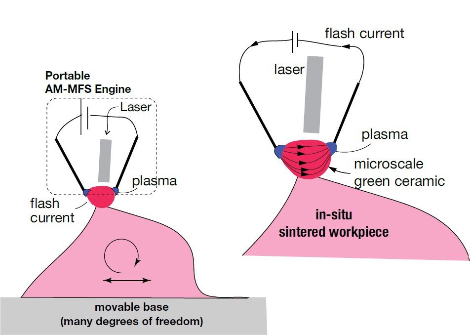
Figure 5. A stand-alone engine for microflash sintering that can be integrated into different types of additive manufacturing systems. Credit: Ingraci Neto and Raj
A schematic of an engine for AM-MFS is illustrated in Fig. 5. A plasma jet can be added to promote contactless electrodes. The engine can be designed as a portable stand-alone system that can be incorporated into various additive manufacturing systems. The spot for flash sintering is heated with the laser. (The heating source can also be a spot-heaters powered by infrared lamps; they are commercially available.) The laser and the electrodes are ganged to one another and adjusted together, in tandem, for microsintering on the surface of the workpiece.
The immediate challenge is the mechanical design and the development of software for system level control of the engine. The voltage and the current must be optimized in the time domain. Simulations and analytical models emerging from manufacturing science would be needed. (An example of such models is presented in Sortino et al.24 for the traveling flash experiment described in Fig. 2). The engine can be evaluated iteratively with model experiments, such as those described by Figures 3 and 4.
Much work lies ahead. But progress can be rapid if emanating from fundamental scientific research in the field of flash and reactive flash sintering.
Acknowledgments
The authors are grateful to the Office of Naval Research, grant N00014-18-1-2270. This research was supported in part by the Colorado Shared Instrumentation in Nanofabrication and Characterization (COSINCCHR) from College of Engineering & Applied Science, University of Colorado Boulder.

Related Articles

Market Insights
Engineered ceramics support the past, present, and future of aerospace ambitions
Engineered ceramics play key roles in aerospace applications, from structural components to protective coatings that can withstand the high-temperature, reactive environments. Perhaps the earliest success of ceramics in aerospace applications was the use of yttria-stabilized zirconia (YSZ) as thermal barrier coatings (TBCs) on nickel-based superalloys for turbine engine applications. These…

Market Insights
Aerospace ceramics: Global markets to 2029
The global market for aerospace ceramics was valued at $5.3 billion in 2023 and is expected to grow at a compound annual growth rate (CAGR) of 8.0% to reach $8.2 billion by the end of 2029. According to the International Energy Agency, the aviation industry was responsible for 2.5% of…

Market Insights
Innovations in access and technology secure clean water around the world
Food, water, and shelter—the basic necessities of life—are scarce for millions of people around the world. Yet even when these resources are technically obtainable, they may not be available in a format that supports healthy living. Approximately 115 million people worldwide depend on untreated surface water for their daily needs,…