
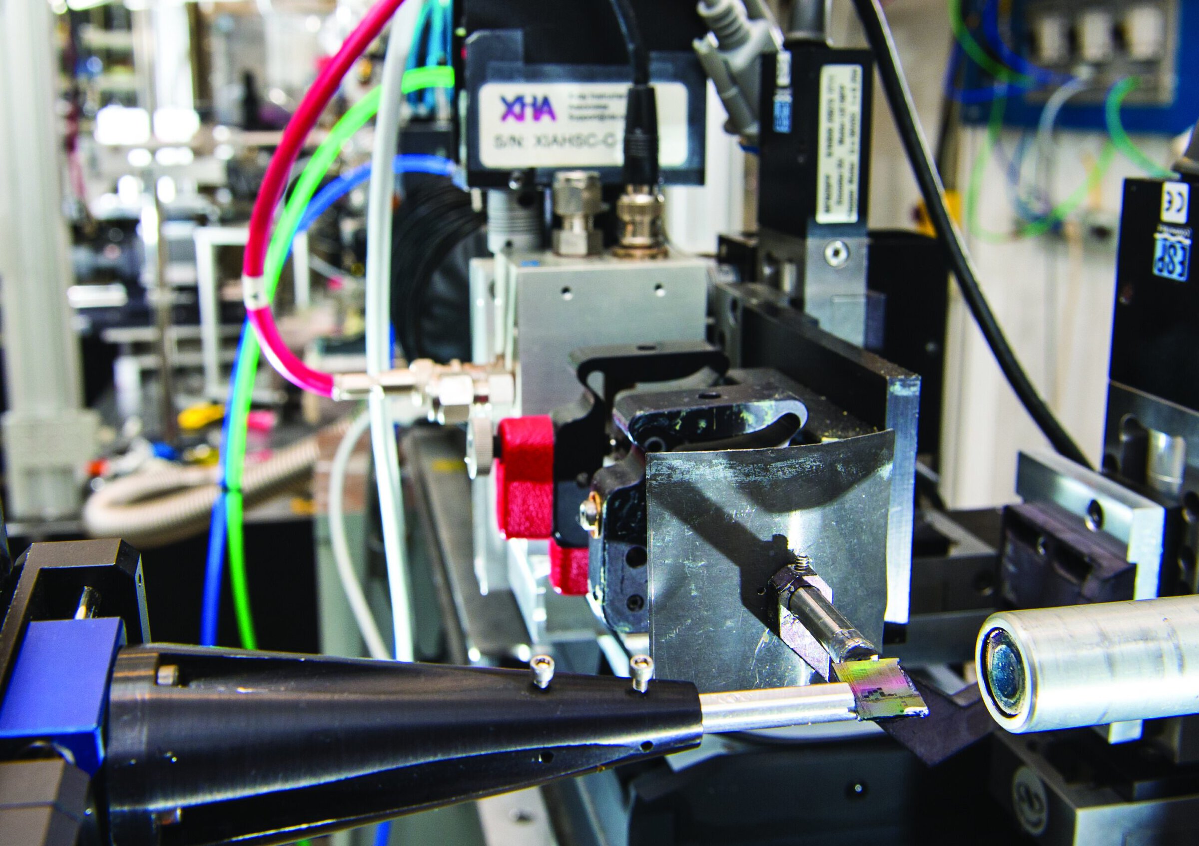
There has been rapid development in the precision with which ferroelectric material can be grown epitaxially on single-crystal substrates and in the range of physical phenomena exhibited by these materials. These developments have been chronicled regularly in the Bulletin.1,2 Ferroelectric thin-film materials belong to the broad category of electronic ceramics, and they find applications in electronic and electromechanical devices ranging from tunable radio-frequency capacitors to ultrasound transducers. The importance of these materials has motivated a new generation of materials synthesis processes, leading to the creation of thin films and superlattices with impressive control over the composition, symmetry, and resulting functionality. In turn, improved processing has led to smaller devices, with sizes far less than 1 micrometer, faster operating frequencies, and improved performance and new capabilities for devices. Important work continues to build on these advances to create materials that are lead-free and that incorporate other fundamental sources of new functionality, including magnetic order.
The polarization of ferroelectric materials can be changed by changing the applied field. (See sidebar below “Piezoelectricity, crystal structure, and symmetry.”) Polarization switching has profound effects on the piezoelectric distortion because the piezoelectric coefficients are effectively reoriented when the polarization is changed. Piezoelectricity is thus an excellent marker for the interplay of mechanical and electronic phenomena responsible for polarization switching.
The thinness, faster operating timescales, and novel structural degrees of freedom available in epitaxial ferroelectric thin films pose difficult challenges for characterization using conventional experimental methods. Researchers have developed a series of powerful—now standard—characterization techniques based on measuring the displacement of the surface of the thin film using piezoelectric force microscopy or interferometry.3 Alternatively, the stress imparted by the piezoelectric material can be quantified using the curvature of the substrate or a cantilever.4 Another approach is to use focused ion-beam milling or selective etching to create a bridge structure or cantilever into the film by removing a section of the underlying substrate and to observe the distortion of the shape of this structure.5 These approaches have proved to be phenomenally successful, but face important limits, particularly regarding time resolution and the precision with which the relationship between atomic-scale effects and the overall electromechanical distortion of the sample can be determined. Understanding the atomic origins of piezoelectricity, particularly at nanosecond time scales, has proved challenging, but new techniques based on X-ray scattering address this void.
X-ray diffraction
X-ray diffractometry techniques provide direct insight into the piezoelectricity of ceramics and epitaxial oxides. Several experimental approaches do this by taking advantage of time-resolved scattering techniques.6–9 For example, X-ray scattering experiments take advantage of the highly brilliant beams of X-rays with tunable photon energy that are available at synchrotron light sources (see “Synchrotron Radiation” section below). The high brilliance of the beam allows for focusing it to small spot sizes. The important aspect of X-ray scattering studies is that the intensity and location in reciprocal space of the reflections provide key information about the functional properties of piezoelectrics. The positions in reciprocal space (derived from the angles at which X-ray reflections appear) provide the lattice constant, and the variations of these positions as a function of the applied electric field determine the piezoelectric coefficients. The strain and diffraction angle are related through the Bragg equation λ = 2dsin θ. Reciprocal space is spanned by wavevectors so that the Bragg reflections occur at wavevectors with magnitude q = 2π/d. The intensity of X-ray reflections depends on the direction of the polarization, an effect that can be combined with nanofocused X-ray beams to produce maps of the direction of the remnant polarization.10
Because X-ray diffractometry allows for precise measurement of lattice parameters, the piezoelectric coefficients can be determined in situ, that is, while the sample is subject to either constant or varying electric fields. Consequently, in situ X-ray diffractometry provides a means to begin understanding the fundamental source of piezoelectric phenomena.
Measuring lattice constants of piezoelectric thin films
Epitaxial thin-film capacitors are an excellent system for testing new ways to probe piezoelectricity. For example, Figure 1 shows the structural changes induced in an epitaxial thin film of BiFeO3 by an electric field pulse lasting 12 nanoseconds.11 The piezoelectric expansion during the electric-field pulse—a strain of approximately 0.5 percent—shifts the diffraction peak to a smaller wavevector, qz. For this measurement, the electric fields were synchronized with X-rays generated by individual bunches of stored electrons at the Advanced Photon Source facility (Argonne National Laboratory, Argonne, Ill.). Thus, the time resolution is limited only by the duration of the X-ray bunches and by the electrical bandwidth of the equipment generating the voltage pulses. The characteristic rise-and-fall times of the shift in the diffraction peak shown in Figure 1 are 1.4 nanoseconds and correspond to the charging time constant of the capacitor. In addition, the shift of the diffraction peak provides a quantitative measure of the variation of the lattice constant during the pulse.
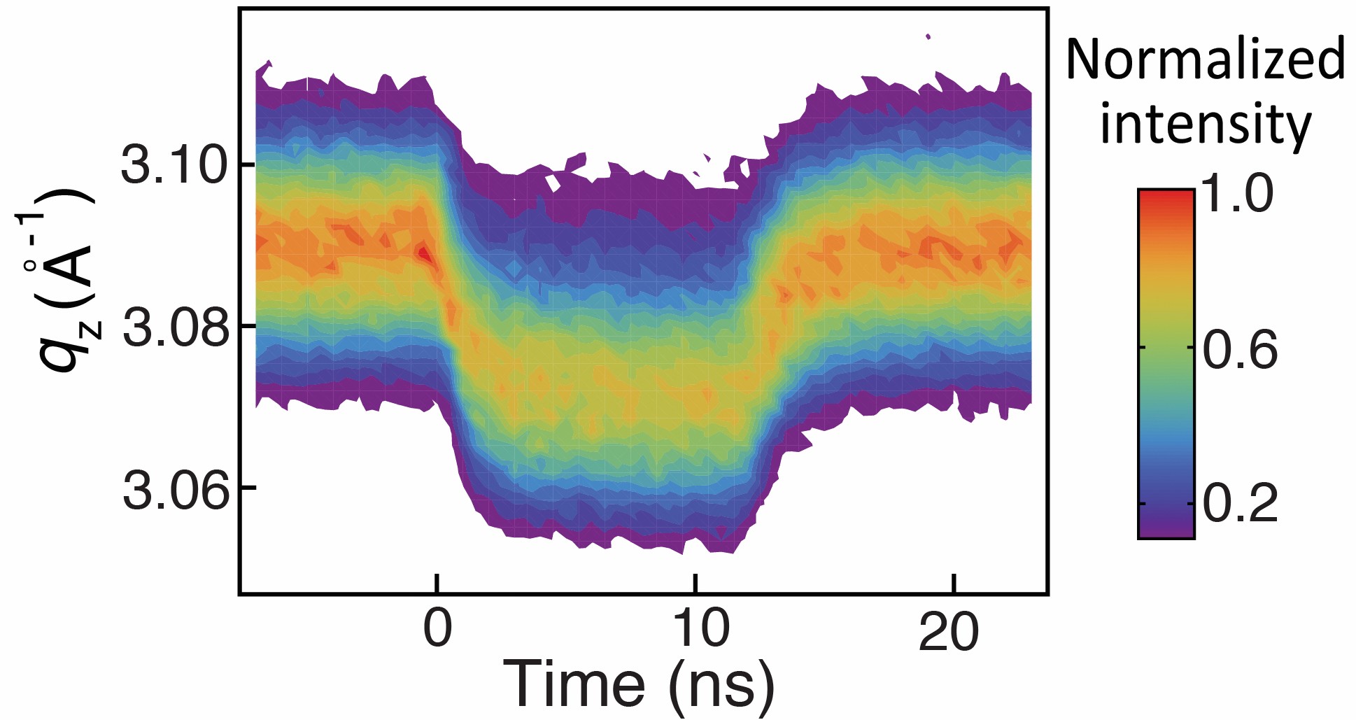
Figure 1. Piezoelectric shift in the wavevector of the 002 Bragg reflection of an [001]-oriented BiFeO3 thin film during an electric-field pulse lasting 12 ns. The wavevector shift corresponds to a piezoelectric strain of ~0.5%.11 Credit: Chen, et al.; American Institute of Physics. Reprinted with permission.
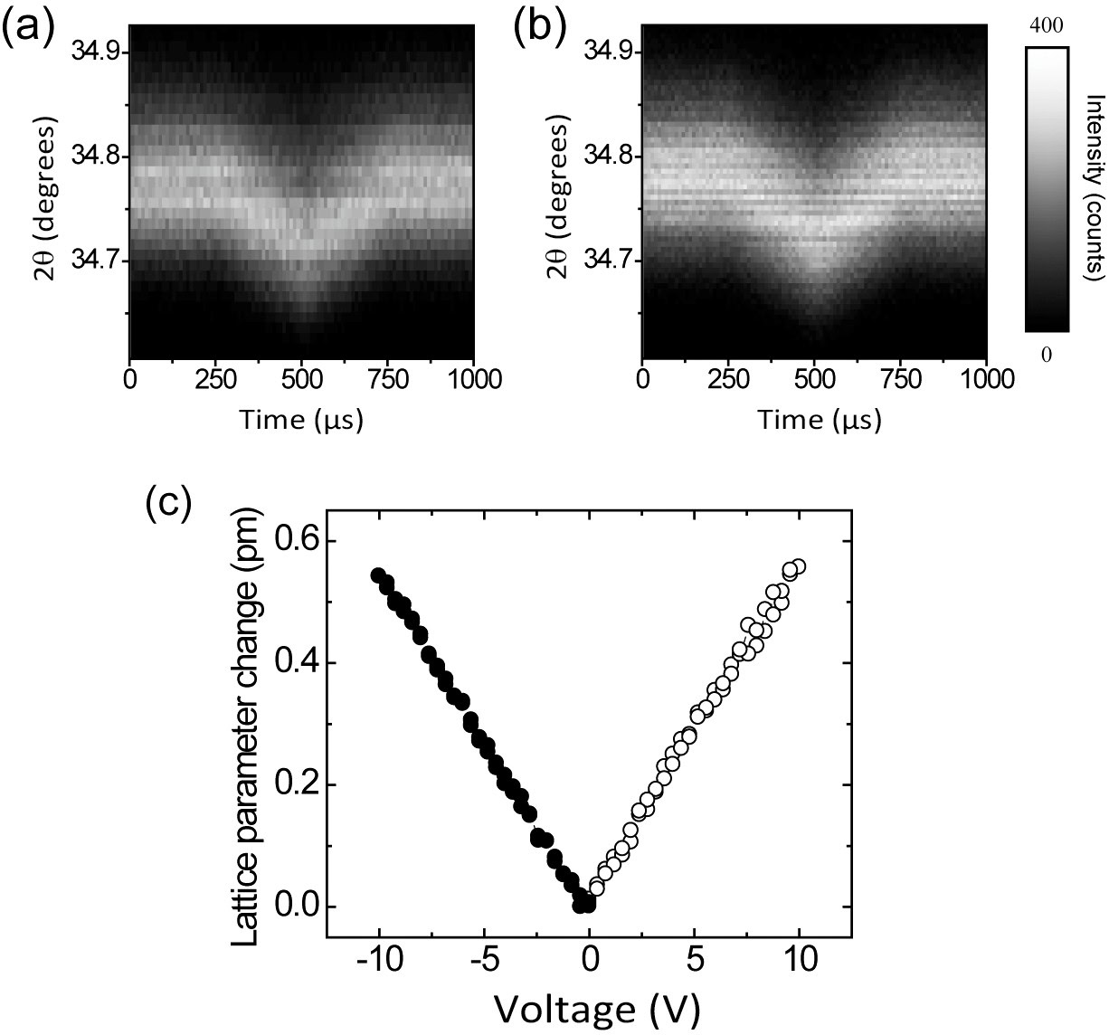
Figure 2. Shift in the 002 Bragg reflection of a Pb(Zr,Ti)O3 thin film in which the top electrode is grounded and (a) positive or (b) negative polarity voltage pulses are applied to the bottom electrode. The reflection shifts to smaller angles, corresponding to larger lattice constants, in both cases because the measurements require many electric-field pulses and the remnant polarization rapidly switches to the direction favored by the sign of the applied field. (c) Field-dependent strain measured from (a) and (b), plotted as a function of the applied voltage. The strain is proportional to the voltage in both cases, with piezoelectric coefficients of 53 pm/V and 54 pm/V for positive and negative voltage pulses, respectively.12 Credit: Do, et al., Taylor & Francis Ltd. Reprinted with permission.
Alternating the sign of applied voltage pulses switches the capacitor between two polarization states in each repetition of the pulse sequence. The diffraction patterns and strain observed in this case are shown in Figures 3(a) and (b). As was the case in Figure 2, large pulses of either sign lead to large piezoelectric expansions. When the voltages switch signs, however, the lattice first contracts, producing the characteristic electromechanical hysteresis shown in Figure 3(b). The results in Figure 3 correspond to a structural observation of the hysteresis of ferroelectric capacitors, an effect that is useful for decoupling the fundamental origin of hysteresis from artifacts associated with electrical measurements.
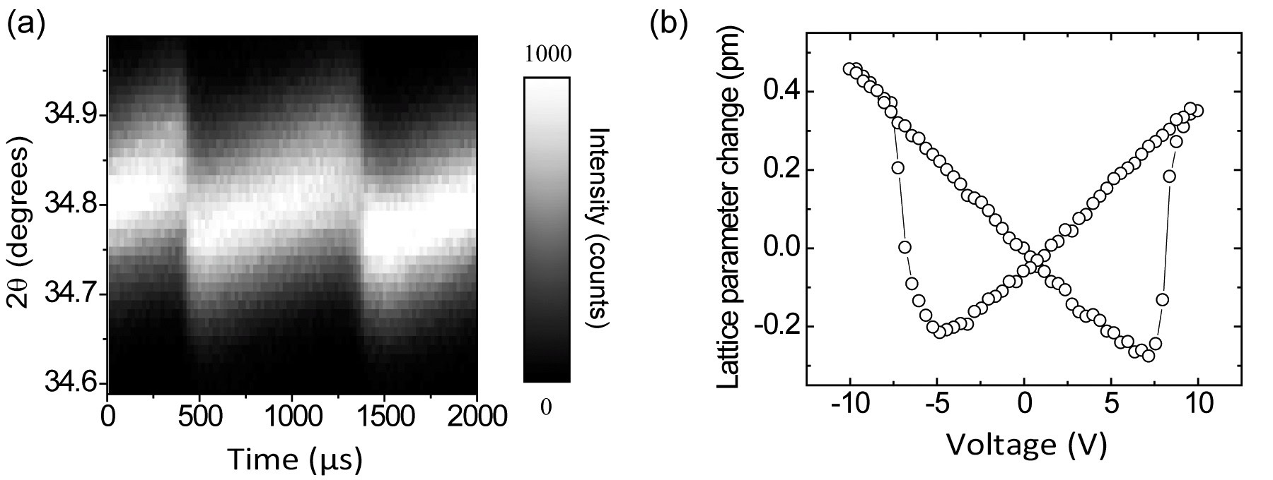
Figure 3. (a) Piezoelectricity-induced angular shift of the 002 Bragg X-ray reflection of a Pb(Zr,Ti)O3 thin film in a bipolar applied electric field. (b) Piezoelectric hysteresis loop derived from (a). These measurements allow the local coercive electric field and piezeoelectric coefficients to be measured.12 Credit: Do, et al., Taylor & Francis Ltd. Reprinted with permission.
Piezoelectricity in thin films with complex microstructures
In Figures 2 and 3, the direction along which the X-ray experiments probed the piezoelectric strain was parallel to the direction of the applied electric field. Thus, the piezoelectric coefficients measured in this case correspond to the d33 component of the piezoelectric tensor. In the thin-film case, only E3 is nonzero, and the piezoelectric coefficients that determine the tensile or compressive strain are d31, d32, and d33. Shear strains are determined by coefficients, d34, d35, and d36. Time-resolved microdiffractometry probes the out-of-plane and the in-plane piezoelectric response, measuring the strains ε1, ε2, and ε3 from changes to the in-plane lattice constants and the out-of-plane c-axis lattice constants, respectively.
The full piezoelectric tensor is particularly important for BiFeO3 because the bulk rhombohedral unit cell is distorted during epitaxial growth, leading to a complex thin-film microstructure.13 Instead of a single intense peak, the {103} reflections of BiFeO3 are split because the film has regions with the four possible orientations of its rhombohedral distortion relative to the cubic substrate, as well as varying degrees of plastic relaxation and tilt. Applying a voltage in this case results in a piezoelectric response that depends on the local structure of the thin film. Figure 4 shows the piezoelectric response by plotting positions in reciprocal space of the BiFeO3 pseudocubic {103} reflections for several electric fields.14 The arrows in Figure 4 indicate the change in reflection positions as E increases from 0 to 250 kilovolts per centimeter. There is no distortion of the electrode material, SrRuO3.
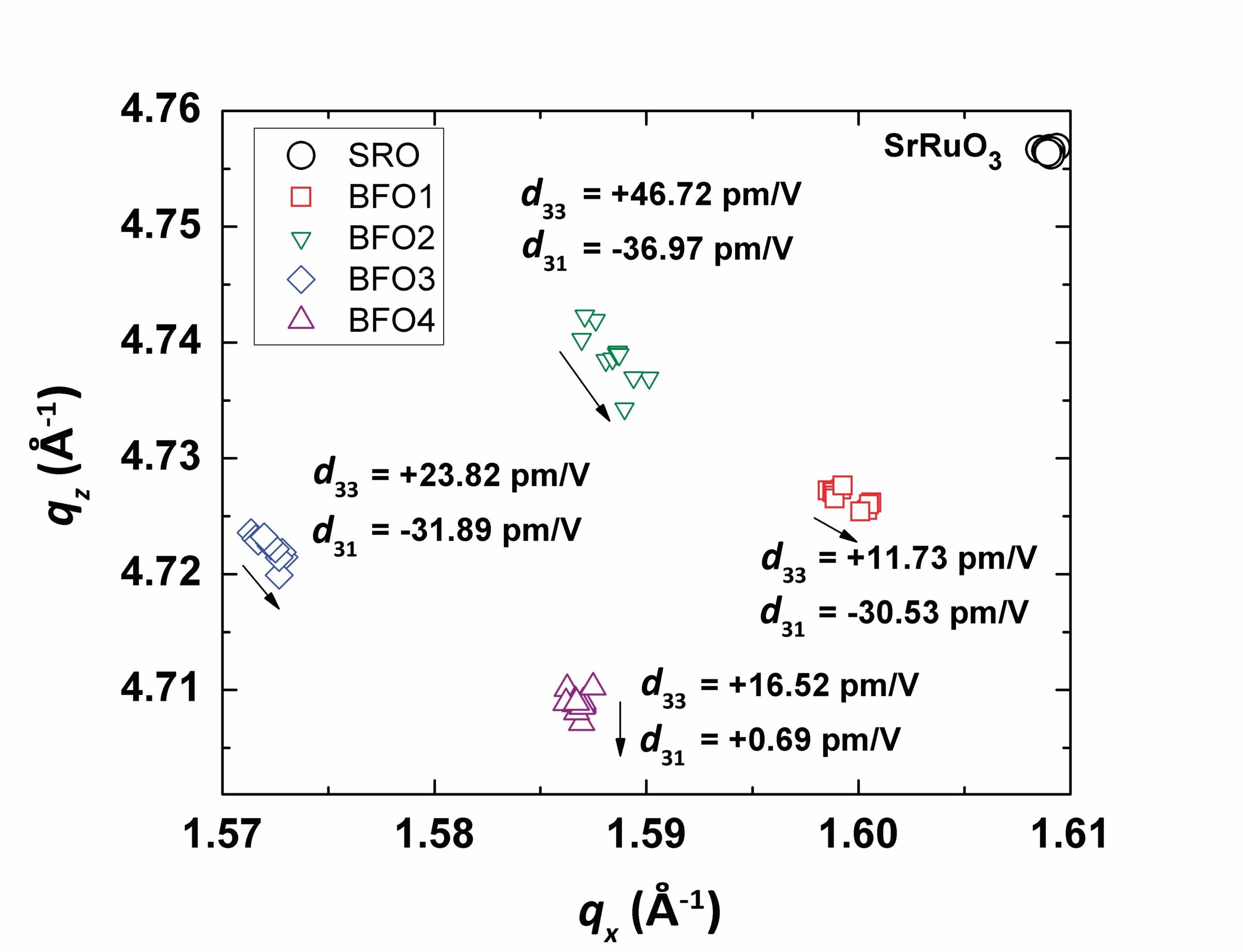
Figure 4. Field-dependent projections of the three-dimensional diffraction pattern of a BiFeO3 thin film onto the qx–qz plane. The BiFeO3 layer exhibits four {103} diffraction peaks, resulting from structural variants with various crystallographic orientation within the X-ray spot. Arrows indicate the directions of the shifts of these reflections in electric fields from 0 to 250 kV/cm. The SrRuO3 reflection is not displaced by the applied field because there is no piezoelectric strain in the bottom electrode.14 Credit: R. Sichel, U. Wisconsin-Madison.
The distortion evident in Figure 4 comes from two closely related effects. The first is the piezoelectric expansion of the lattice. A second, more subtle effect, is the rotation of the {103} planes as the c lattice constant increases, which rotates the peak position around the origin in reciprocal space. The values of d33 and d31 for each distinct structural volume, shown next to the reflections in Figure 4, do not account for rotations of the atomic planes and represent only the apparent change in lattice constant. Nevertheless, it is clear that the piezoelectric response varies for each domain. The apparent value of d31 domains at this location on the sample ranges from –37 picometers per volt to +0.69 picometers per volt. The nonzero values of d31 occur because the in-plane lattice constant within the domains is not completely clamped by the substrate, and each domain is in a different stress states because of the incomplete relaxation of the film. A domain near the edge of a mosaic block or any other type of defect, for example, is under mechanical constraints very different from one in a perfectly epitaxial region of the film.
The in-plane piezoelectric response of the partially relaxed BiFeO3 lies between the polycrystalline and epitaxial regimes. A completely clamped film would have an effective d31 of zero. Wafer flexure studies have shown that polycrystalline Pb(Zr,Ti)O3 thin films grown by the sol–gel method have values of d31 that increase with increasing film thickness, probably because the substrate clamps the film less effectively as the film gets thicker.4 BiFeO3 domains with nonzero d31 are likely to be in the more relaxed regions than in regions with no in-plane piezoelectric response. These effects are even more pronounced in ceramics, where in situ diffractometry studies have shown that the fraction of the overall piezoelectric distortion that directly results from the expansion of the lattice is small compared with the motion of domain walls and other long-range elastic effects.7
High fields, ultrafast dynamics, and complex domains
The precision and high resolution of in situ diffractometry probes provide a way to study electromechanical materials in new regimes, such as ultrashort pulses or very large electric fields. The ability to apply short-duration electric-field pulses allows materials to be studied in electric fields with magnitudes far larger than fields at which the film would exhibit dielectric breakdown in steady state. These high fields can reach 2 to 3 megavolts per centimeter and lead to strains of 2.0 percent in BiFeO3 and up to 2.7 percent in Pb(Zr,Ti)O3.11, 15 These fields can be large enough that the approximations that the strain and electric field are small no longer apply. For BiFeO3, in particular, the effects that result from high fields are particularly large, as shown in Figure 5.11 In this case, the electric field is applied along the pseudocubic [001] direction of a BiFeO3 thin film, leading to a large strain consistent with the rotation of the polarization and the possibility that the system is approaching a structural rhombohedral-to-tetragonal phase transition. Such phase transitions have been reported in thin films grown with varying degrees of epitaxial mismatch,16 but diffractometry probes have not yet been able to capture the transitions or their dynamics in situ.
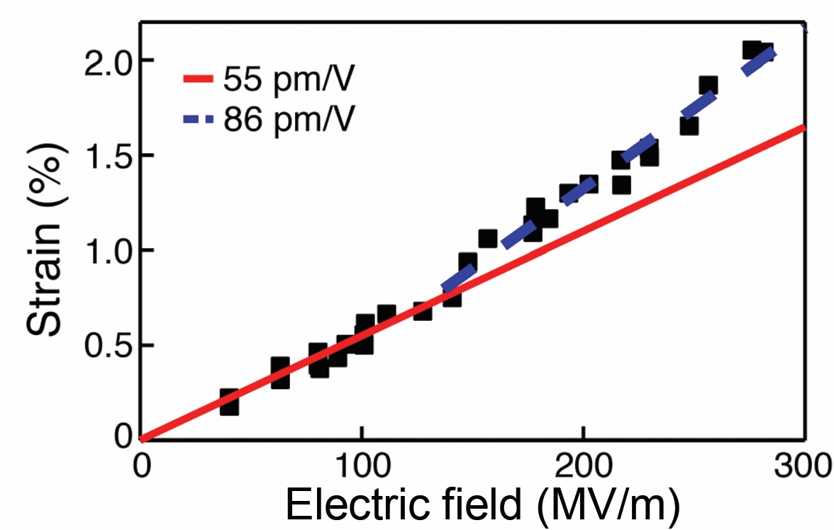
Figure 5. Electric-field dependence of the piezoelectric strain in BiFeO3 thin films at very high electric fields. The low-field piezoelectric coefficient of 55 pm/V does not provide a good fit to strains observed at fields above ~150 MV/m.11 Credit: Chen, et al.; American Institute of Physics. Reprinted with permission.
A further use of the time resolution of in situ techniques is in understanding the intrinsic time scales of the processes responsible for the electronic properties of ferroelectrics. In epitaxial ferroelectrics, polarization switching occurs by a process in which domains of the polarization favored by the field nucleate and grow across the film. This process can be imaged stroboscopically by using the large piezoelectric expansion that occurs when the polarization switches as a marker for the transition. The images reveal that domains in a PZT thin film nucleate with characteristic spacings of several micrometers and subsequently propagate into the unswitched material at a velocity of 40 meters per second under electric fields of 230 kilovolts per centimeter.6
Diffractometry probes are particularly useful when the thin film has a complex domain pattern. For example, epitaxial superlattices consisting of alternating layers of dielectric and ferroelectric materials spontaneously form a nanometer-scale striped domain pattern that results because of the weak interaction between adjacent ferroelectric layers.17 An applied electric field can favor stronger coupling, enough to drive the system into a single-polarization state. In this situation, diffraction information comes from the domains themselves and from the piezoelectric strain induced by applied electric fields, as shown in Figure 6.19 Insight into the mechanism of the electric-field-induced transformation from the striped-domain state to the eventual uniform polarization state can be obtained either at long timescales using laboratory X-ray diffractometry17 or at nanosecond elapsed times using synchrotron-based techniques.18
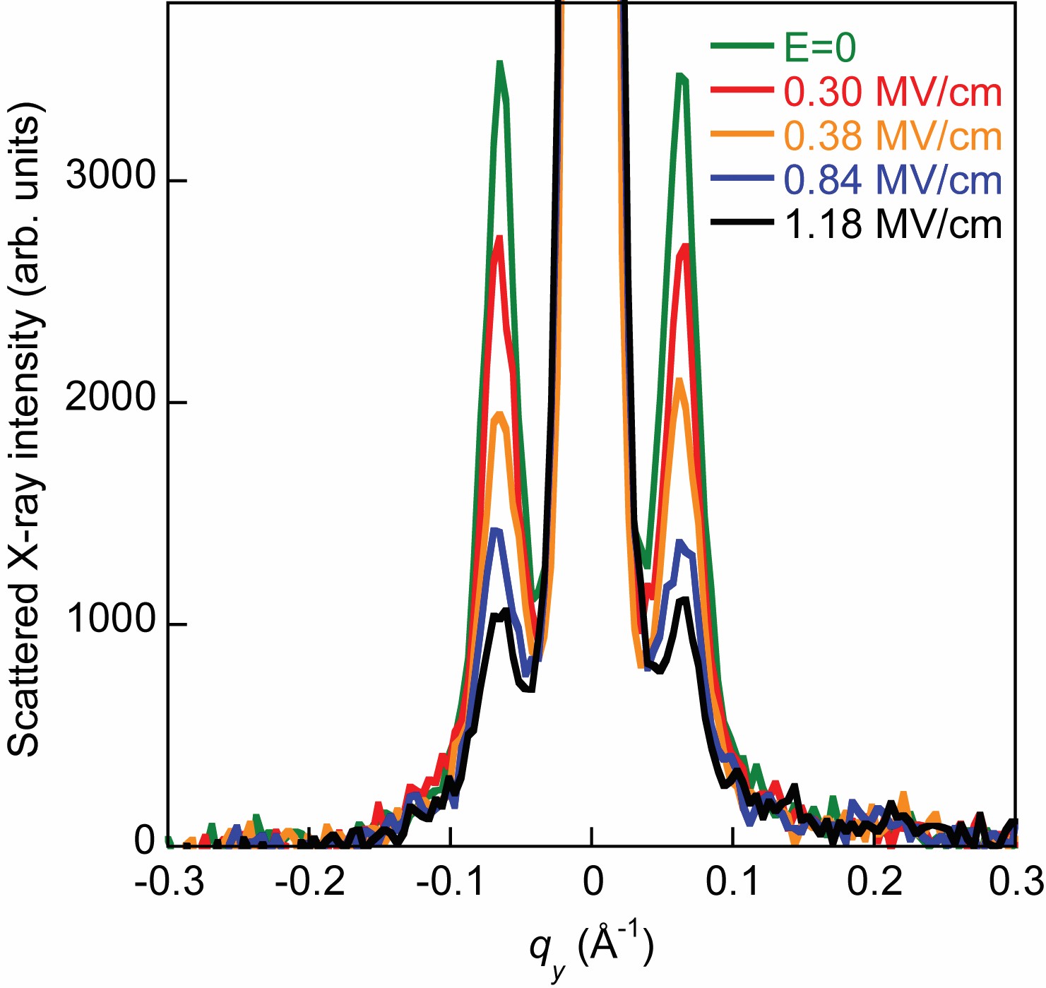
Figure 6. Disappearance of domain satellite reflections at Qy = 0.08 Å–1 in a PbTiO3/SrTiO3 superlattice in an applied electric field. The decrease in the intensity of these satellites occurs because the applied field drives the system out of the striped domain state and into a configuration with uniform polarization in the SrTiO3 and PbTiO3 layers. Credit: Evans; U. Wisconsin-Madison.
Outlook
In situ diffractometry studies offer a quantitative way to characterize the properties of piezoelectric materials and to begin to understand the fundamental origin of these properties. The precision with which lattice parameters can be measured in X-ray studies allows piezoelectric coefficients to be extracted quantitatively for thin-film materials, in the conventional case where the films expands normal to the surface and when adjacent areas cooperatively vary their in-plane structures. In more complex systems, in situ probes allow the properties of piezoelectrics to be studied at high electric fields, very short pulse times, and in systems with unusual domain patterns. Further applications of this approach will allow researchers to better understand the relationship between piezoelectric properties and crystallographic symmetry, for example, in testing theoretical predictions of the role of distortions of oxygen octahedra in superlattice materials.19 Advances in X-ray technology will allow these studies to extend to shorter picosecond-scale times, and with improvements in X-ray detectors, to probe less-well-ordered systems including polymers and other organic piezoelectrics.
Acknowledgments
The authors gratefully acknowledge support from the Ceramics Program of the NSF Division of Materials Research through grants DMR-0705370 and DMR-1106050. The authors also thank Pice Chen, Alexei Grigoriev, Ji Young Jo, and Dal-Hyun Do for collaborations and insightful discussions.
Piezoelectricity, crystal structure, and symmetry—The piezoelectric coefficients
Piezoelectricity results from the polarization of crystals lacking inversion symmetry. In these materials, an applied stress leads to a change in the electrical polarization, and, conversely, applied electric fields lead to a change in the lattice constants, referred to as the piezoelectric strain. In the limit of small strains, fields, and stresses, the piezoelectric strain is proportional to the applied electric field, and the strain tensor and electric field are related by εjk = dijk∙Ei, where ε is the strain tensor, d is the piezoelectric coefficient, and E is the applied electric field vector.20 Note that the piezoelectric tensor can lead to strains and shears along directions that are orthogonal to the applied field. The units of d, more properly referred to as the converse piezoelectric coefficient, are distance divided by potential difference, often given in picometers per volt. The three-index notation for the piezoelectric coefficient can be reduced to a two-index notation, dij, where the index i refers to the electric field direction in the conventional manner where 1, 2, and 3 refer to the x, y, and z directions, respectively. The second index j refers to elements of the strain tensor using Voigt notation.20 The tensor of converse piezoelectric coefficients dij relates the piezoelectric strain εj to the electric field Ei:

The symmetry of thin films and ceramics is such a strong effect that a second, engineering notation, is widely used in describing the piezoelectric coefficients. The notation and units are identical to the ones described above, which can lead to some confusion about which definition is in use. In the engineering notation, piezoelectric coefficients are defined so that the z direction, corresponding to subscript 3, is always in the direction of the applied electric field. Thus, the expansion along the field direction is determined by the piezoelectric coefficient d33 in the engineering notation. The symmetry of the piezoelectric tensor also is different between the two definitions. In the crystallographic definition, the piezoelectric tensor has the symmetry of the crystallographic unit cell. In the engineering definition, the tensor has the same symmetry as the overall shape of the piezoelectric thin film or ceramic solid, which is quite different from the crystallographic symmetry.
The multiferroic complex oxide bismuth ferrite BiFeO3 is an excellent example of the difference between the crystallographic and engineering definitions of piezoelectricity. Although BiFeO3 has rhombohedral symmetry in bulk crystals, a pseudocubic notation for the BiFeO3 piezoelectric tensor and X-ray reflections are often used to emphasize the epitaxial relationship between the BiFeO3 thin film and its cubic substrate. The rhombohedral symmetry of BiFeO3 is not apparent from this notation, which has the side effect of complicating the expression for the piezoelectric tensor. Projecting the piezoelectric tensor onto the [100], [010], and [001] directions of a tetragonal material forces most of the terms to be zero and makes many of the remaining coefficients identical.20
Synchrotron radiation
Third-generation X-ray sources from synchrotron light sources, such as the Advanced Photon Source at Argonne National Laboratory (Argonne, Ill.), generate X-rays with very high intensity and small angular divergence, termed “brilliance.” This brilliance, in turn, allows X-rays to focus to very small spot sizes, on the order of 100 nm or smaller. This spatial resolution is comparable to scanning probe microscopy and makes the study of the functional properties of highly heterogeneous materials possible.
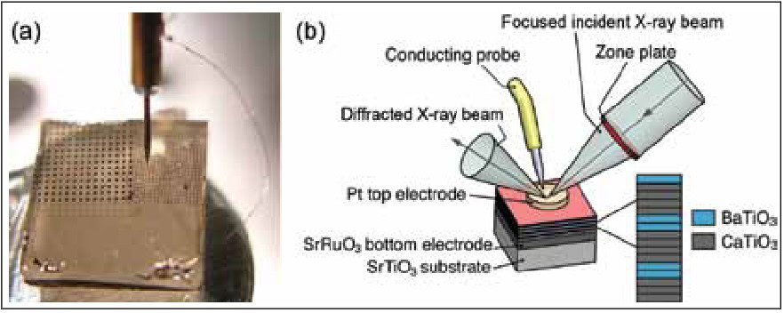
(a) Photograph and (b) schematic of in situ synchrotron X-ray diffractometry studies of piezoelectric materials. The sample shown schematically in (b) is a heteroepitaxial superlattice consisting of alternating layers of BaTiO3 and CaTiO3.20 Credits: (a) Alexei Grigoriev, Univeristy of Tulsa; (b) Chen et al.; IOP. Reprinted with permission.
X-ray wavelengths are selected to match the needs of the experiment. Wavelengths of ~1 Å, which are required for diffractometry experiments, easily penetrate the top electrodes of device structures, such as capacitors, which allows in situ studies to be performed in applied electric fields. Even with the angular convergence introduced by focusing, synchrotron X-ray diffractometry experiments have sufficient precision to observe piezoelectric strains on the order of 10–5. In these studies of piezoelectricity, the thin-film capacitor is positioned at the focus of the X-ray beam and the diffractometry experiment is conducted in an electric field provided by a probe tip contacting the top electrode.

Related Articles

Market Insights
Next-gen superconducting ceramics could change how we travel and much more
Forty years ago, two physicists from IBM’s research laboratory in Zürich, Switzerland, reported a groundbreaking discovery: Superconductivity, or the quantum mechanical phenomenon in which certain materials exhibit zero electrical resistance when cooled, could be achieved at higher temperatures using ceramics. Superconductivity had been discovered decades before, but its applications had…

Market Insights
Why most AI manufacturing projects fail and how to fix it
Artificial intelligence is reshaping advanced manufacturing, especially processes involving ceramics, glasses, and other hard or brittle materials. But adopting AI is far more difficult than simply buying software and connecting machines. Manufacturers must understand the advantages and limitations of different models, so they can determine where AI fits best within…

Bulletin Features
Radiation effects on rare earth chemistry in molten salts for nuclear applications
Across the nuclear energy sector, molten salts are shaping the next generation of nuclear technologies, from advanced power reactors to used nuclear fuel recycling. In molten salt reactors (MSRs), molten salts uniquely serve as both the primary coolant and fuel medium, a dual role that sets MSRs apart from conventional…