

Chalcogenide glasses (ChGs) refer to a broad family of inorganic amorphous materials containing one or more of the Group IV chalcogen elements, namely sulfur, selenium, and tellurium. Although these glasses carry an exotic name compared with their oxide counterparts (e.g., silica glass), they are veteran players on the microelectronics industry stage, functioning as the main constituent material for phase change memory (PCM).
PCM technology takes advantage of the relative ease of transforming ChGs, in particular glasses in the Ge-Sb-Te (GST) composition group, between their glassy and crystalline states to store digital information. Gordon Moore, in 1970, building on pioneering work by Ovshinsky et al., coauthored a groundbreaking article featuring the first ChG-based memory—at that time, a 256-bit device1. This was five years after Moore predicted the now-famous Moore’s Law. Since then, PCM technology has evolved from a mere laboratory curiosity to a series of cutting-edge nonvolatile memory modules marketed by major companies, including Samsung, Micron, and IBM (Figure 1a). Besides their phase changing behavior, ChGs also are well-known for their exceptional optical properties, including broadband infrared (IR) transparency and large optical nonlinearity, making them popular materials for IR optical components such as windows, molded lenses, and optical fibers (Figure 1b).
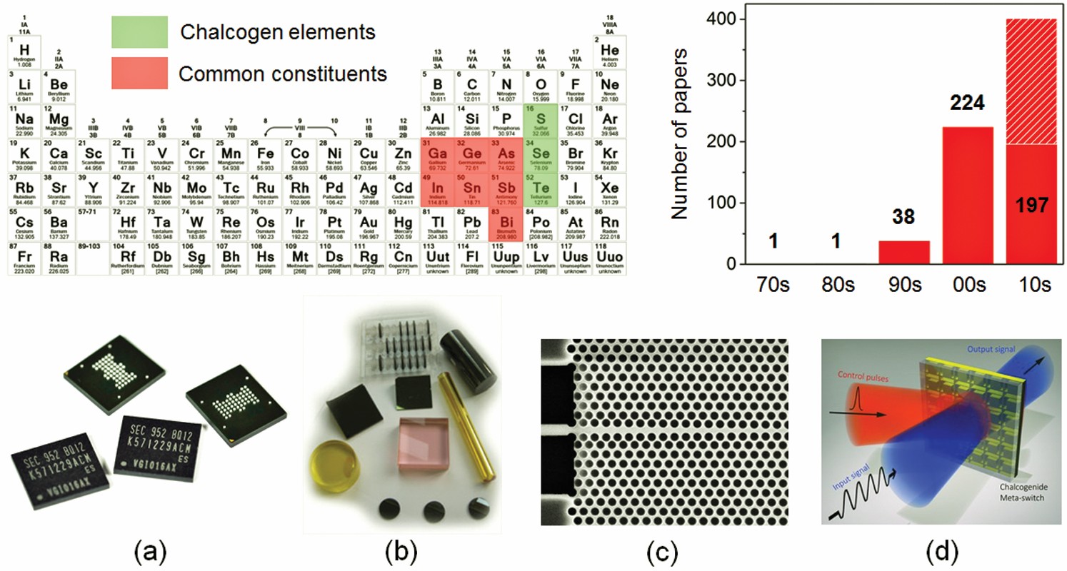
Figure 1. Top left: The periodic table highlighting chalcogen elements (green) and other common constituent elements in ChGs (red). Top right: number of publications with keywords “chalcogenide glass” and “photonic/optical device” found in the Web of Science database. (a) Phase change memory inside multi-chip packages. (b) ChG IR molded lenses, IR windows, and fiber preforms.* (c) Photonic crystal waveguide embedded in a suspended ChG membrane. Hole diameter is 260 nm.† (d) Metamaterial switch operating on phase change behavior of ChGs.**
*Image courtesy of Wei Zhang, Ningbo University, China
†Image courtesy of Steve Madden, Australian National University
**Image courtesy of B. Gholipour et al., Adv. Mater., 25[22], 3050–3054 (2013) Credit: Hu
Burgeoning interest has been catalyzed by many material and device technology advances that overcome some aforementioned drawbacks of ChG materials. Chemically and structurally stable glasses with arsenic-free compositions now are routinely prepared in both bulk and thin-film forms using techniques readily scalable to high-volume production, such as microwave synthesis, chemical vapor deposition, and solution processing.3,4 Leveraging standard semiconductor processing methods, such as plasma etching or nanoimprinting,5,6 high-quality photonic components were demonstrated with optical propagation loss down to 0.05 dB/cm.7 Emerging applications, including nonlinear all-optical signal processing, chem-bio sensing, and on-chip light switching and modulation (Figure 1(c) and 1(d))—all of which exploit the unique optical characteristics of ChGs—are being actively pursued.8
Flexible photonics
Some shortcomings of the glasses, however, are more difficult to circumvent because they are inherent to chalcogenide materials. For instance, ChGs consist of atoms larger than atoms comprising oxide glasses, which makes the interatomic bonds weaker and limits mechanical performance. Mechanical strength of bulk ChGs further deteriorates from the presence of defects, such as inclusions, microcracks, and voids. Therefore, the term “flexible chalcogenide glass photonics” appears to be an oxymoron. It seems counterintuitive to choose ChGs as the backbone optical material for photonic integration on flexible polymer substrates, which must sustain extensive deformation such as bending, twisting, and even stretching.
Setting aside mechanical properties, ChGs exhibit a number of features that outclass rival materials when it comes to photonic integration on flexible substrates. First of all, unlike crystalline materials that typically require epitaxial growth to form thin films, amorphous ChGs can be coated directly onto plastic substrates using a plethora of well-established vapor- or solution-phase deposition techniques. Consequently, ChG-based photonic devices can be monolithically fabricated on flexible substrates.
This is in stark contrast with conventional flexible photonic integration, which generally relies on single-crystal silicon for low-loss light guiding. This material choice dictates a multi-step transfer fabrication process that initially fabricates devices on a sacrificial layer (usually silica), followed by chemically dissolving the sacrificial layer to release the devices, picking up the floating devices using a poly(dimethylsiloxane) rubber stamp, and finally, transferring them onto the flexible receiving substrate.9,10
Instead, using amorphous chalcogenide materials, we deposit and pattern photonic structures directly on flexible substrates. In the world of microfabrication, where “simple is better,” this simplified monolithic integration approach significantly improves device processing quality, throughput, and yield. Also, the temperature for processing ChG films is compatible with the limited thermal budget stipulated by the polymer substrate. ChG films can be patterned into functional photonic devices at reduced temperatures (typically below 200°C) without compromising the resulting thin film’s optical performance, thanks to weak interatomic bonds in chalcogenide compounds and, hence, reduced glass transition and softening temperatures. As an added benefit, the low processing temperature mitigates CTE mismatch between ChGs and substrates. Last but not least, high refractive indexes of ChGs (typically 2 to 3) offer strong confinement of light by total internal reflection inside microsized waveguide devices, which facilitates compact photonic integration on a chip-scale platform.
The current challenge is to devise a new device architecture that takes advantage of these attractive features of ChGs for flexible photonic integration without being handicapped by their mechanical fragility. The Hu research group at Massachusetts Institute of Technology and coauthors teamed with the Nanshu Lu group at University of Texas at Austin to develop a “multi-neutral-axis” design schematically illustrated in Figure 2(a). According to the design, the polymer substrate assumes a laminated “Oreo” geometry consisting of three layers: a soft elastomer layer with a typical Young’s modulus in the few MPa range sandwiched between two stiff epoxy films with Young’s modulus of the order of several GPa.
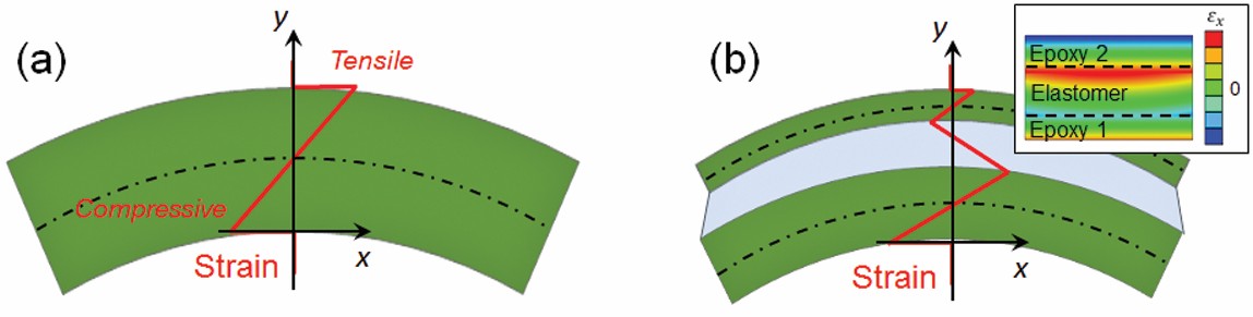
Figure 2. Bending of (a) a simple uniform beam and (b) a sandwiched “Oreo” structure with large elastic mismatch. Strain distributions inside the layers are superimposed on the plots. Inset (b) shows a contour plot of strain distribution inside a trilayer structure computed using the finite-element method. Credit: Hu
The large three-orders-of-magnitude modulus mismatch between the layers causes bending strains to be largely absorbed by the elastomer layer so that strains inside epoxy layers are effectively relieved when the composite structure is bent. The hypothesis is validated through finite-element numerical simulations. Figure 2(b) inset shows a contour plot of bending strain distribution inside such a sandwich structure, where strains concentrate in the elastomer layer. Further theoretical analysis11,12 reveals that the classical Kirchhoff assumptions that describe stress and deformation in thin plates no longer hold in laminates, such as these, composed of materials with drastically different elastic properties.
Strain distribution in the sandwiched structure follows a zigzag pattern across the laminate thickness and exhibits multiple neutral planes where the strains vanish (Figure 2(b)). When photonic devices are positioned at the neutral planes, strains exerted on the devices are nullified even if the multilayer structure deforms, thereby rendering the structure extremely flexible. More importantly, the locations of neutral planes can be configured as desired across the stack thickness by tuning layer thicknesses and elastic moduli. Therefore, laminate design enables rational control of strain–optical coupling in flexible photonic structures and allows large degrees of freedom for photonic device placement to meet diverse application needs.
Figure 3(a) shows the process to fabricate flexible photonic components with the sandwiched structure shown in Figure 2(b). The process starts with spin coating an epoxy polymer layer onto a rigid handler substrate, usually silicon wafers coated with oxide. The polymer-coated handler wafer provides a solid, planar support on which to pattern photonic devices, leveraging standard microfabrication techniques similar to those used for computer-chip manufacturing. The preferred composition for this application is Ge23Sb7S70 (GSS) glass. Although GSS glass is a close relative of GST, replacing tellurium with the glass-former sulfur significantly improves thermal and structural stability of the glass against crystallization. Single-source thermal evaporation13 is used to deposit the GSS film. The substrate is held at room temperature throughout the deposition process. A second epoxy layer, whose thickness is chosen to locate devices at the neutral plane, is subsequently deposited. In the last step, devices embedded inside the epoxy layer are delaminated from the handler substrate using polyimide-film tape (in this case, Kapton Tape by DuPont) to form a free-standing, flexible photonic chip shown in Figure 3(b). The bilayer polyimide-film tape consists of a polyimide substrate and a silicone adhesive layer. The final flexible chip has the desired structure, with a soft silicone layer sandwiched between two stiff epoxy-and-polyimide layers.
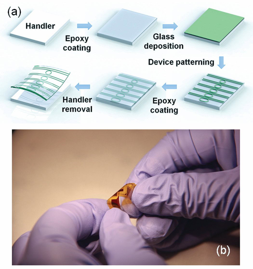
Figure 3. (a) Fabrication process for ChG flexible photonic devices. (b) Example of a flexible photonic chip.11 Credit: Hu
ChG flexible photonic devices fabricated using this approach considerably outperform their traditional counterparts in optical characteristics, mechanical robustness, and processing throughput and yield. Light propagation loss inside flexible devices was quantified by measuring optical transmission characteristics of microdisk resonator structures, which are miniscule optical reservoirs capable of trapping light via multiple total internal reflections in a closed path—in the same way that sound waves cling to the walls of the whispering gallery at St. Paul’s Cathedral in London.
Resonators are characterized by an important parameter called “quality factor” or “Q-factor,” which scales inversely with optical loss inside the devices. Our monolithic fabrication route offers extremely high device yields. We have tested over 100 resonator devices randomly selected from samples fabricated in several batches. All operated as designed after fabrication. The Figure 4(a) histogram shows distribution of Q-factors in the flexible resonators measured near 1,550-nm wavelength. Our best device exhibited a Q-factor as high as 4.6 × 10⁵, the highest value ever reported for photonic devices on plastic substrates. To test the mechanical reliability of the flexible devices, optical transmittance of the resonators was measured after repeated bending cycles with a bending radius of 0.5 mm. Figure 4(b) shows that there were minimal variations in Q-factor and extinction ratio after multiple bending cycles. Our fatigue test, consisting of up to 5,000 bending cycles at a radius of 0.8 mm, resulted in a 0.5 dB∙cm–1 increase in waveguide propagation loss and a 23% decrease in resonator Q-factor. Optical microscopy revealed no crack formation or interface delamination in the layers after 5,000 bending cycles.11 These results demonstrate the superior mechanical robustness of ChGs-based flexible devices. In comparison, traditional flexible photonic components exhibit only moderate flexibility with bending radii typically no less than 5 mm.
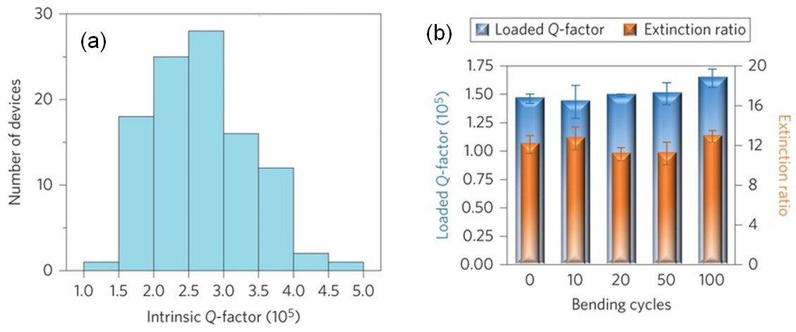
Figure 4. (a) Q-factor distribution measured in flexible microdisk resonators. (b) Q-factors and extinction ratios of the resonator after multiple bending cycles at a bending radius of 0.5 mm.11 Credit: Ref 11
The flexible photonics platform opens many emerging application opportunities. For example, biophotonics capitalizes on mechanical flexibility to facilitate photonic system interfacing with soft biological tissues. For photonic system assembly, flexible components are ideal for space-constrained packaging. On the manufacturing side, flexible photonics integrate seamlessly into large-area roll-to-roll production processes. We also have harnessed device mechanical flexibility to demonstrate reconfigurable photonics, where a component’s optical response can be tuned by controlled deformation. For example, a focusing-dispersive element with tunable focal length was realized by attaching a flexible diffractive grating to surfaces with various curvatures (Figure 5).
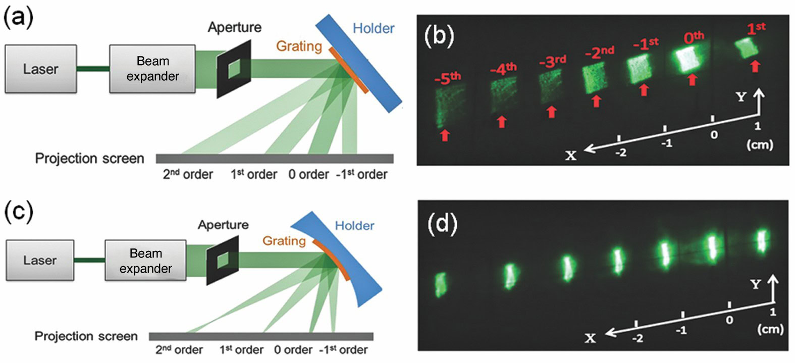
Figure 5. (a) and (c) Schematic diagrams illustrating the experimental setup used to map diffraction patterns from flexible gratings that were attached onto (a) a flat sample holder and (c) a curved sample holder. (b) and (d) Diffraction patterns of a collimated and expanded 532-nm green laser beam by gratings mounted on (b) a flat surface and (d) a curved surface. (Images courtesy of Y. Zou, et al., Adv. Opt. Mater. 2, 759-764 (2014)). Credit: Zou, et al.
Chemical sensors
Flexible photonics represent a case in point where we capitalize on glasses’ low-temperature monolithic deposition and processing capacity to enable photonic integration on unconventional substrates. We can extend the approach to other functional substrates, which is another advantage of ChGs over conventional photonic materials such as silicon, silica, or LiNbO3. Conventional optical materials have to be grown either epitaxially (for crystalline materials such as silicon and LiNbO3) or at high temperatures (silica) that are incompatible with flexible substrate materials. In another example that showcases the “substrate-blind” integration paradigm, we demonstrated a ChG-on-CaF2 platform for mid-infrared spectroscopic sensing of chemical species. Silica and polymers, the classical material choices for waveguide claddings, become opaque in the mid-IR range (4–10 μm). ChGs, on the other hand, exhibit low optical loss across the mid-IR band, which qualifies them as ideal material candidates for IR spectroscopic sensors.14–17 For example, GSS glass transmits in the 0.6–11 μm wave band. To expand the accessible wavelength regime of glass-based photonic devices, we chose CaF2, an IR crystal with a low index of refraction (n=1.4) and a broad transparency window of 0.3–8 μm, as the substrate material in place of silica or polymers.
In our mid-IR sensing demonstration, we again elect high-Q-factor glass optical resonators for spectroscopic sensing. Their unique ability to store photons for an extended period of time leads to a folded optical path that can be several orders of magnitude longer than the device’s physical dimensions, thereby significantly boosting interactions between light and target molecules to be detected. During operation, optical absorption from the molecules results in attenuation of light circulating inside the resonators and signals the presence of target species in the sensing medium to which resonators are exposed. The wavelength and line shape of measured absorption spectra identify the molecule type, whereas optical absorption strength quantifies molecular concentration.
Similar to the flexible photonics device fabrication process, glass-on-CaF2 resonators were prepared by thermal evaporation of GSS glass film onto CaF2 substrates followed by lithographic patterning to define sensor structures. Figure 6(a) shows a top-view micrograph of a microdisk resonator made of GSS glass on CaF2 coupled to a feeding waveguide. Optical characteristics of these devices were interrogated using a tunable quantum cascade laser (QCL) in the 5.2∙5.4-μm mid-IR band (Figure 6(b)). Measurement revealed a high Q-factor up to 4 × 10⁵ in the resonators (Figures 6(c) and 6(d)), which corresponds to a low propagation loss of 0.26 dB∙cm–1 and represents the best performance attained in on-chip mid-IR resonators. Such a low optical loss contributes to increased optical path length inside the device and, thus, is critical to improve the sensitivity of spectroscopic detection.
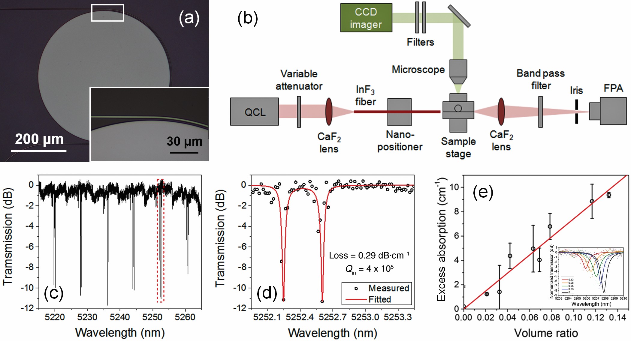
Figure 6. (a) Top-view micrograph of a GSS-on-CaF2 microdisk resonator. Inset shows the coupling region between feeding waveguide and microdisk. (b) Experimental setup used to measure mid-IR optical transmission through glass-on-CaF2 sensor devices. (c) Mid-IR transmission spectrum of a micro-disk resonator. (d) The same spectrum near an optical resonance at 5252 nm wavelength (red box in (c)). Open circles represent experimental data, whereas the solid line is the doublet-state resonance spectrum fitted by coupled mode theory, which yields an intrinsic Q-factor of 4 × 10⁵ and an equivalent propagation loss of 0.29 dB·cm–1. (e) Optical resonance decreases with increasing ethanol concentration. (images courtesy of Reference 14 authors). Credit: Ref 14
To demonstrate proof-of-concept, we immersed the resonator sensor in ethanol–cyclohexane solutions of varying ethanol concentrations while monitoring the resonator optical response in situ. Ethanol exhibits a weak absorption feature at 5.2 μm wavelength (relative to its main IR absorption band at 3.9 μm, which has a peak absorption coefficient of 2900 cm–1), whereas cyclohexane is almost transparent at the wavelength.18
When ethanol concentration increased, we observed a progressive decrease of optical resonance intensity (Figure 6(e) inset). Thus, we infer the excess optical absorption induced by ethanol (Figure 6(e)). The absorption coefficient of ethanol in cyclohexane was extrapolated by a linear fit of the plot to be (74 ± 3.4) cm–1, which agrees well with measurement results (78 cm–1) obtained on a bench-top Fourier transform infrared spectrophotometer. The resonator-enhanced sensing mechanism readily can be generalized to spectroscopic analysis of other biological and chemical species in the mid-IR.
Tuning functionality with multilayer devices
Flexible glass-on-polymer and glass-on-CaF2 platforms discussed so far involve only single-layer photonic devices. The substrate-blind integration strategy, however, can be extended to process even more complex stacked multilayer structures, again thanks to the amorphous nature and low processing temperature of ChGs, which minimize thermal and structural mismatch between different layers. Using a repeated deposition-patterning-planarization sequence illustrated in Figure 7(a), we successfully demonstrated an array of multilayer photonic devices, such as add-drop optical filters, adiabatic interlayer couplers, and 3-D woodpile photonic crystals.11 For example, Figure 7(b) shows a tilted-view scanning electron microscopy cross-sectional image of a woodpile photonic crystal fabricated using this approach.
The photonic crystal comprises four layers of GSS glass strips (marked with various colors) embedded inside an epoxy polymer, where the strip pattern is rotated in-plane by 90° between consecutive layers to form a tetragonal lattice structure. To study structural integrity of the photonic crystal, a collimated 532-nm green laser beam was incident on the photonic crystal. Figure 7(c) shows diffracted light spots, the optical analog of the Laue pattern in X-ray crystallography. Excellent agreement between diffraction spot locations predicted by the Bragg diffraction equation and experimental measurements confirmed long-range structural order in the photonic crystal.
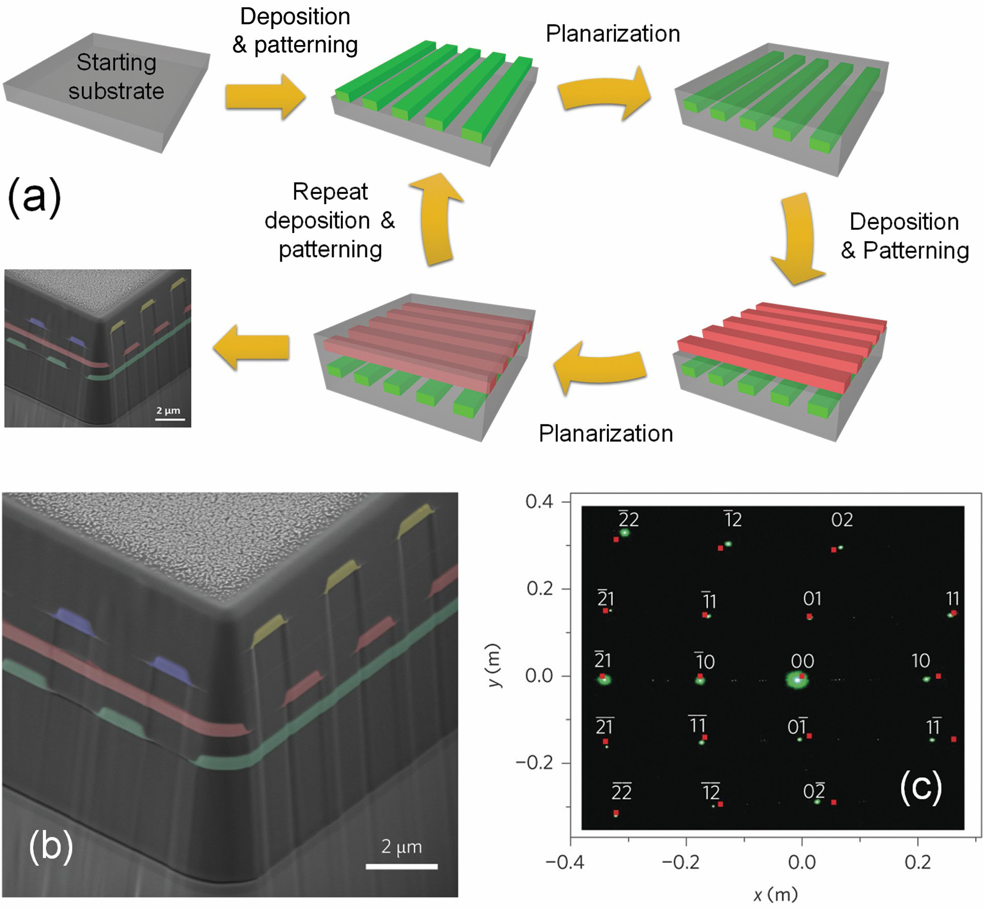
Figure 7. (a) Process flow of multilayer photonic structures in ChG films. (b) Tilted SEM view of a 3-D woodpile photonic crystal showing excellent structural integrity. (c) Diffraction patterns of a collimated 532-nm green laser beam from the photonic crystal. Red dots are diffraction patterns simulated using the Bragg diffraction equation.11 Credit: Ref 11
To realize such novel function beyond single layers and to be able to tune functionality in the z-direction, the team examined strategies to design and fabricate passive and active (doped) layers using film processing routes that maintain dopant dispersion. Recent efforts investigated a novel approach based on aerosols of glass solution to create spatially defined single and multilayer structures that are compatible with the variety of substrates discussed previously. In electrospray film deposition of ChGs, a solution is atomized into a fine mist of relatively monodispersed droplets through an electric field. This deposition method has the potential to fabricate graded refractive index (GRIN) coatings by tailoring the index of subsequent coating layers, using a 3-D printing-like approach via two simple methods. First is the separate deposition of two oppositely sloped (shaped) films of various ChG compositions using a computer numerical control system that controls motion between substrate and spray. Second is the use of multiple spray heads.
Unexplored potential of ChGs
We have shown how we use ChG materials’ processing versatility, broadband optical transparency, and monolithic integration capability to enable novel microphotonic functionalities, such as flexible photonics, IR spectroscopic sensing, and multilayer integration. Through smart material engineering, processing design, and device innovation, we have overcome challenges traditionally linked with ChGs. For example, substituting arsenic with germanium and tellurium with sulfur improves the chemical and structural stability of chalcogenides against oxidation and crystallization while reducing the components’ toxicity. Low processing temperature coupled with appropriate choice of bottom cladding material minimizes CTE mismatch and prevents delamination in multilayer structures. The multi-neutral-axis device design allow us to create photonic components out of brittle glasses yet bestow on them extreme mechanical flexibility, a feature polymers claimed almost exclusively in the past.
This article reveals only the tip of the iceberg compared with what ChG materials have to offer the microphotonics field.
Examples of exciting new applications not covered in this article include nonlinear optical interactions in ChGs for ultrafast all-optical signal processing on a chip,19 photosensitivity in glasses (a useful attribute for device fabrication), and postfabrication trimming.20 Our groups are exploring monolithic and hybrid integration of chalcogenide devices with 2-D materials (e.g., graphene), III-V semiconductor devices, and complex oxides to broaden the glass microphotonic platform’s functionality. We foresee that ChGs also will make their way into semiconductor integrated photonic circuits to confer unique optical functions, such as IR transmission, nonlinearity, or trimming by incorporating the materials into a photonic chip manufacturing process. This follows the same trend we observed in the microelectronic integrated circuit industry, which initially used only a handful of elements in the 1980s but now has assimilated more than half the Mendeleev periodic table into the manufacturing process to keep pace with Gordon Moore’s prediction. Now it is time to see if ChGs—the magic materials that underlie another of Moore’s seminal inventions—will be able to make their mark on microphotonics in coming years.
Capsule summary
Properties help and hinder
Chalcogenide glasses offer unique optical properties that oxide glasses cannot, such as broadband infrared transparency and optical nonlinearity. However, compositions can be toxic and mechanical properties are poor.
Breakthrough
Versatile techniques for depositing chalcogenide glass thin films and clever device structure design provide new, scalable pathways for fabricating devices.
Payoff
Integrating chalcogenide glasses on a range of substrates opens the possibility to design innovative devices, such as flexible photonics and on-chip infrared spectroscopic sensors, with broad optical functionality.

Related Articles

Market Insights
Next-gen superconducting ceramics could change how we travel and much more
Forty years ago, two physicists from IBM’s research laboratory in Zürich, Switzerland, reported a groundbreaking discovery: Superconductivity, or the quantum mechanical phenomenon in which certain materials exhibit zero electrical resistance when cooled, could be achieved at higher temperatures using ceramics. Superconductivity had been discovered decades before, but its applications had…

Market Insights
Why most AI manufacturing projects fail and how to fix it
Artificial intelligence is reshaping advanced manufacturing, especially processes involving ceramics, glasses, and other hard or brittle materials. But adopting AI is far more difficult than simply buying software and connecting machines. Manufacturers must understand the advantages and limitations of different models, so they can determine where AI fits best within…
Bulletin Features
Radiation effects on rare earth chemistry in molten salts for nuclear applications
Across the nuclear energy sector, molten salts are shaping the next generation of nuclear technologies, from advanced power reactors to used nuclear fuel recycling. In molten salt reactors (MSRs), molten salts uniquely serve as both the primary coolant and fuel medium, a dual role that sets MSRs apart from conventional…