

Piezoelectric materials are the key functional component in many devices, such as sensors, actuators, ultrasonic transducers, sonar systems, and energy scavengers. These applications take advantage of the direct or reverse piezoelectric effects caused by simultaneous shifts in positive and negative charge centers within the primitive unit cell in response to mechanical deformation.
Ideal piezoelectric materials also are perfectly dielectric. However, most piezoelectric materials are wide bandgap semiconductors that have a finite amount of free charges. The polar field resulting from the direct piezoelectric effect naturally interacts with charged species present in the solid in a Coulombic manner, and, thus, influences charge carrier distribution throughout the solid. This interaction also exists in many widely used semiconductors that are piezoelectric, such as ZnO, GaN, and CdS. Nevertheless, this polar field–charge interaction effect long has been overlooked by piezoelectric and semiconductor researchers until the recent emergence of the field known as piezotronics.1
Piezotronics is a new field that deals with the coupling of piezoelectric polarization (Ppz) with semiconductor properties to design new devices with novel functionalities and enhanced capabilities (Fig. 1). The general principle of piezotronics lies on the Ppz-induced internal and external free charge redistribution that can tune the local interfacial band structure and, thus, provide a mechanism to engineer the charge transport properties without altering the interface structure or chemistry.2-4 In a heterojunction, the effect of the energy state discontinuity is profound, with electronic transport properties that are exquisitely sensitive to the magnitude of the discontinuity. It then follows axiomatically that the electronic properties of the heterojunction system can be tailored by precise modification of the interfacial energetics. To that end, Ppz could have a significant influence on the heterostructure’s electronic properties.
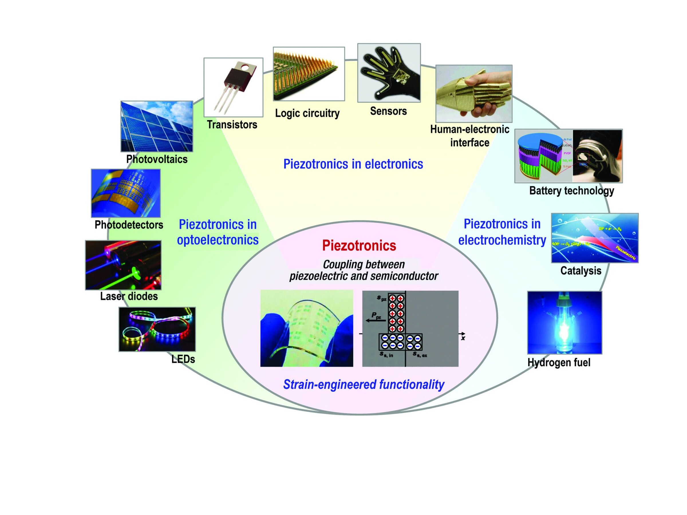
Figure 1. The new field of piezotronics couples the piezoelectric and semiconducting properties of materials to engineer strain-induced functionality into a wide range of new and familiar materials. Credits: (a) Ma; U. Wisc–Madison; (b) Wolf Technical Services for USAF; (c) Wang; U. Wisc–Madison; (d) Wikipedia
In 2006, the piezotronic phenomenon was first demonstrated in a Ppz-gated ZnO nanowire (NW) transistor.5 The great promise of the piezotronic principle has been explored since then in a variety of semiconductor systems as a means for gating transistors, switching diodes, augmenting the quantum efficiency of light-emitting diodes (LEDs), improving photovoltaic (PV) performance, and optimizing catalytic ability.6 This emerging field has quickly attracted researchers worldwide from a wide range of disciplines, including materials science, physics, chemistry, electrical engineering, and mechanical engineering. This article outlines the basic principles, current research progress, and promising future of the new, interdisciplinary research field of piezotronics.
Minding the gap—Semiconductor band engineering
In a heterojunction structure involving a piezoelectric semiconductor material, the appearance of piezoelectric polarization will lead to a considerable change of free charge distribution in the piezoelectric material and its adjacent semiconductor or metal contacts.3 For example, in the p-n junction shown in Fig. 2(a), the original interfacial band structure results from charge redistribution caused by Fermi-level mismatch. Because one of the junction materials is piezoelectric, straining creates immobile piezoelectric charge (σpz) at the piezo-material surface. The free charge concentrations in both junction-forming materials are finite. Therefore, free charges with an opposite sign to σpz (that is, screening charge) are attracted to the interface internally from the piezo-material (σs,in) and externally from the contacting material (σs,ex) (the bottom picture of Fig. 2(a)). The sum of σs,in and σs,ex is typically equal or very close to σpz, and the relative ratio between σs,in and σs,ex is determined by the material’s carrier concentrations and density of states. The net charge gain at the interface (σpz – σs,in) at the piezo-material side, and σs,ex at the non-piezo side) creates additional potential profile at the interface (top curves of Fig. 2(b)).
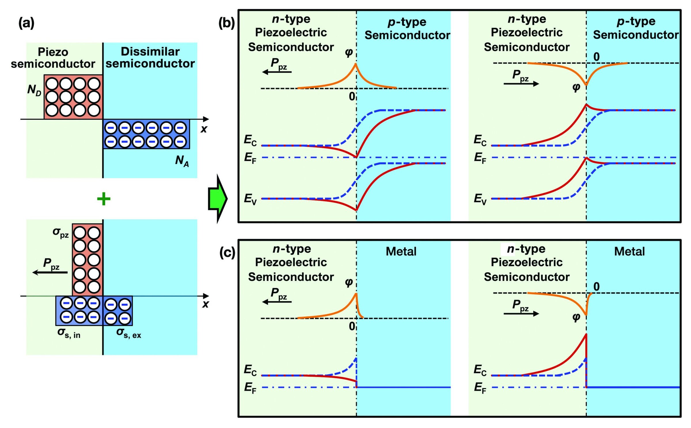
Figure 2. (a) Schematic charge distribution at semiconductor hetero-interface (top) and Ppz-induced charge redistribution (bottom). (b) and (c) Band structure change as a result of the combination of intrinsic and Ppz-induced charge distributions when the piezo-material is (b) n-type semiconductor and the other material is p-type semiconductor or (c) metal. Credit: Wang
Figure 2(b) illustrates the effect of Ppz on the p-n junction. The original band structure is shown by blue dashed lines, and the band structure modulated by Ppz is sketched in red solid lines. The left and right diagrams, respectively, illustrate situations of positive and negative σpz at the interface. Superimposing the Ppz-induced potential profile onto the original semiconductor band structures resolves the shifted band structure. The greatest band shifting exists at the interface, whereas the band structure remains unchanged far from the interface. With this modification, the built-in potentials and depletion regions in both materials change. Figure 2(b) demonstrates a situation where the σpz is so large that it completely inverts the band tilting direction at the n-type piezo-semiconductor side (for positive σpz, left picture) or the p-type non-piezo-semiconductor side (for negative σpz, right picture).
Metal–semiconductor (MS) heterojunctions are another large category of solid-state devices. Here, the screening length in metal is negligible compared with the semiconductor. Therefore, the Ppz-induced band shifting occurs only on the semiconductor side. Figure 2(c) illustrates a MS Schottky junction. Positive σpz at the MS interface reduces the Schottky barrier height. If σpz is large enough, the Schottky barrier can become ohmic (left picture in Fig. 2(c)). When negative σpz appears at the MS interface, the barrier height is more pronounced and creates a Schottky diode with higher threshold voltage.
The existence of Ppz is a steady-state effect as long as the strain is held, although the screening charges prevent external detection of a piezopotential.4 Therefore, applying strain to a piezo-semiconductor constantly influences the band structure as described, and it offers an effective strategy to modulate the performance of practical heterojunction-based devices.
New transistor and sensor devices—Memory switches and artificial skin
The most direct application of the Ppz–band structure relationship presented in Fig. 2 is its modulation of charge transport through the piezoelectric material, that is, a piezotronic transistor. In a piezotronic transistor, the piezoelectric potential induced by strain replaces the conventional gate voltage. This configuration requires only two electrical terminals (electrodes) and is much simpler than regular electrically gated transistors. This is a great advantage for system miniaturization and 3D integration, for example, incorporating vertical NW arrays that can be individually addressed and controlled.
The first piezotronic transistor based on a single crystal ZnO microwire (MW) was demonstrated in 2006.5 Through in-situ bending and I–V characterization in a scanning electron microscope chamber, a monotonic reduction of source-drain current was observed when the deflection generated a piezopotential along the MW’s side wall. This work marked the first discovery of the piezotronic effect and quickly led to further research that involved more comprehensive characterization and obtained deeper understanding of the piezotronic phenomenon. For example, using a ZnO NW, Zhou et al. demonstrated a strain-induced I–V characteristic change in a Ag–ZnO–Ag system consisting of back-to-back Schottky barriers (Fig. 3(a)).7 This system can be represented by the MS model shown in Fig. 2(c), where both electrodes share the same magnitude but opposite sign of potential change at the interface. This produces asymmetrical I–V curves, which makes it possible to use the M1–S–M2 structure as a memory switch.
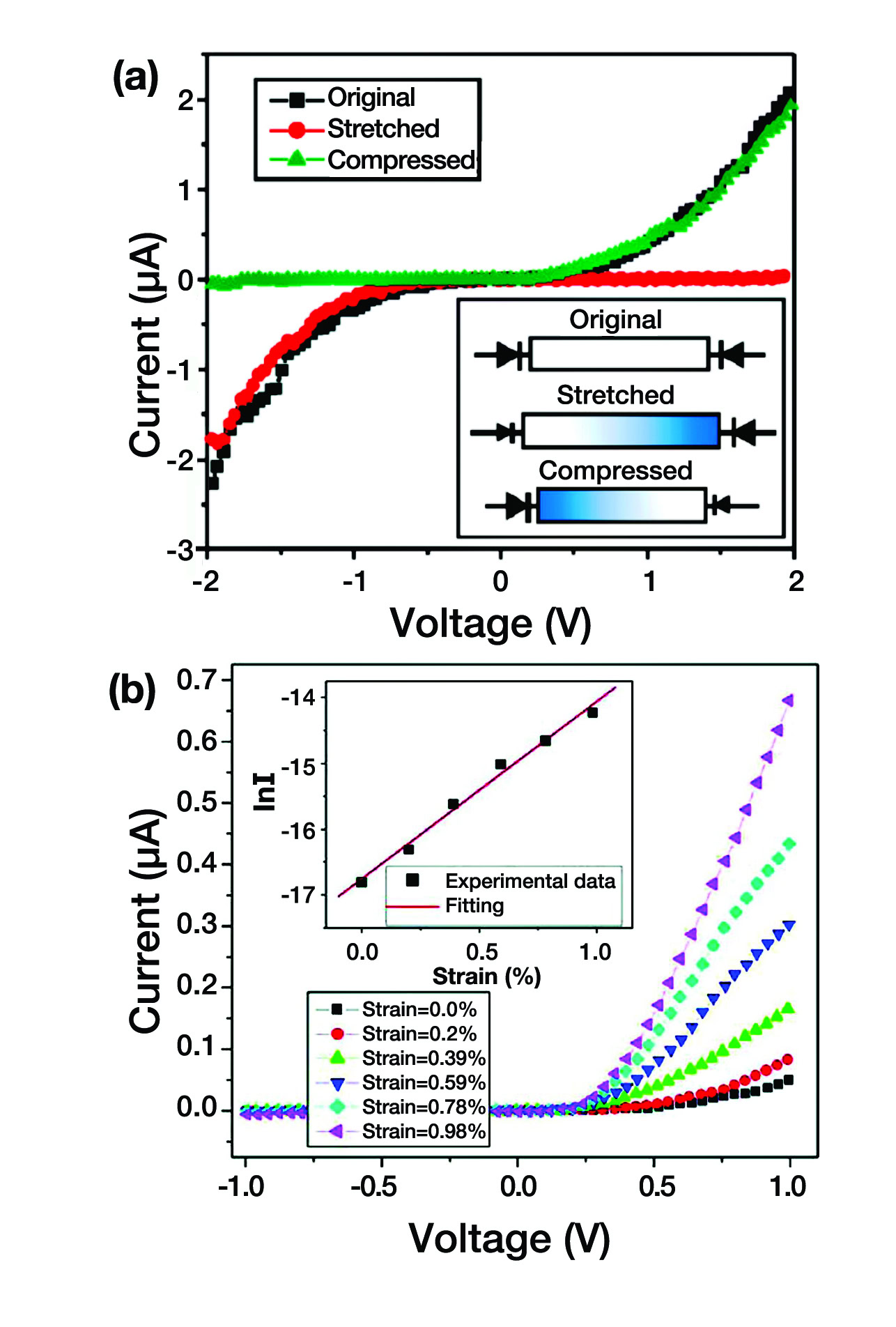
Figure 3. (a) I–V characteristics of a Ag–ZnO–Ag system under zero, compressive, and tensile strains. (b) Strain-sensing performance of the Ag–ZnO piezotronic device. Part (a) adapted with permission from Reference 8. Copyright 2008, American Chemical Society. Part (b) adapted with permission from Reference 7. Copyright 2008, American Chemical Society.Credit: (a) Zhou et al., Nano Lett.; (b) Zhou et al., Nano Lett.
Intuitively, strain sensors are a direct application of the strain-regulated conductivity change. Different from the piezoresistivity, which is a bulk property and typically follows a linear relationship with strain, the piezotronic effect controls the interface barrier height, and, thus, the current change follows an exponential relationship with strain (Fig 3(b)). As a result, a piezotronic strain sensor offers a much enhanced gauge factor (the ratio between current change and strain amplitude). The highest reported gauge factor from a piezotronic ZnO NW was about 1250.8 This value significantly exceeds the gauge factors of commercial semiconductor strain sensors (~100–200) and the highest gauge factor reported for carbon nanotubes (~1000).
Because of their high sensitivity and simple configuration, NW piezotronic strain sensors represent an ideal solution for artificial skin and human–electronic interfaces. Most recently, Wu et al. developed a large-area flexible piezotronic sensor sheet using individually addressed vertical ZnO NW-bundle arrays.9 When subjected to external force or pressure, Ppz was generated at the ZnO–metal contact interface and modulated the barrier height. Thus, the sensitivity was improved by a factor of at least 30 compared with resistive devices. The sensor array provided shape-adaptive force–pressure imaging with a very high resolution of 8,464 pixel/cm2, which is more than an order of magnitude higher than mechano-receptors in the skin of human fingertips (~240 /cm2). This transparent and flexible force–pressure sensor sheet is able to mimic the sense of human skin and offers a novel platform for interfacing human body and electronics.
Similar to regular transistors, piezotronic transistors also can be used for logic circuits, where the on–off states are switched by strain-induced Ppz. Wu et al. demonstrated that multiple ZnO NW–Ag Schottky junctions that were integrated and operated by straining could perform universal logic operations, including NAND, NOR, and XOR.10 Such mechanically operated logic units offer a new function component for advanced nanoelectromechanical systems.
Working with light—Piezophototronics and piezotronic-enhanced photovoltaics
Piezophototronics involves modulation of optoelectronic phenomena by engineering the band structure using the piezotronic effect. The basic principle also follows the diagram shown in Fig. 2, where the amplitude of band shifting at a heterojunction is controlled by strain to manipulate charge recombination (for light-emitting devices) or separation (for photovoltaic devices) at the junction.
Yang et al. reported a dramatic improvement in the emission intensity of an n-ZnO MW/p-GaN-based LED by straining the ZnO MW component (Fig. 4).11 This is the case of p-n junction modulation described in Fig. 2(b). In this configuration, Ppz-induced interfacial charge redistribution forms a potential dip at the ZnO–GaN interface, which traps electrons or holes and facilitates their recombination. Similar to LEDs, in the case of a GaN–InGaN quantum well laser, the quantum well profile can be rectified by Ppz at the well’s interface.12 Whether there is a negative or positive effect on the quantum efficiency results depends on the polarity of this potential.
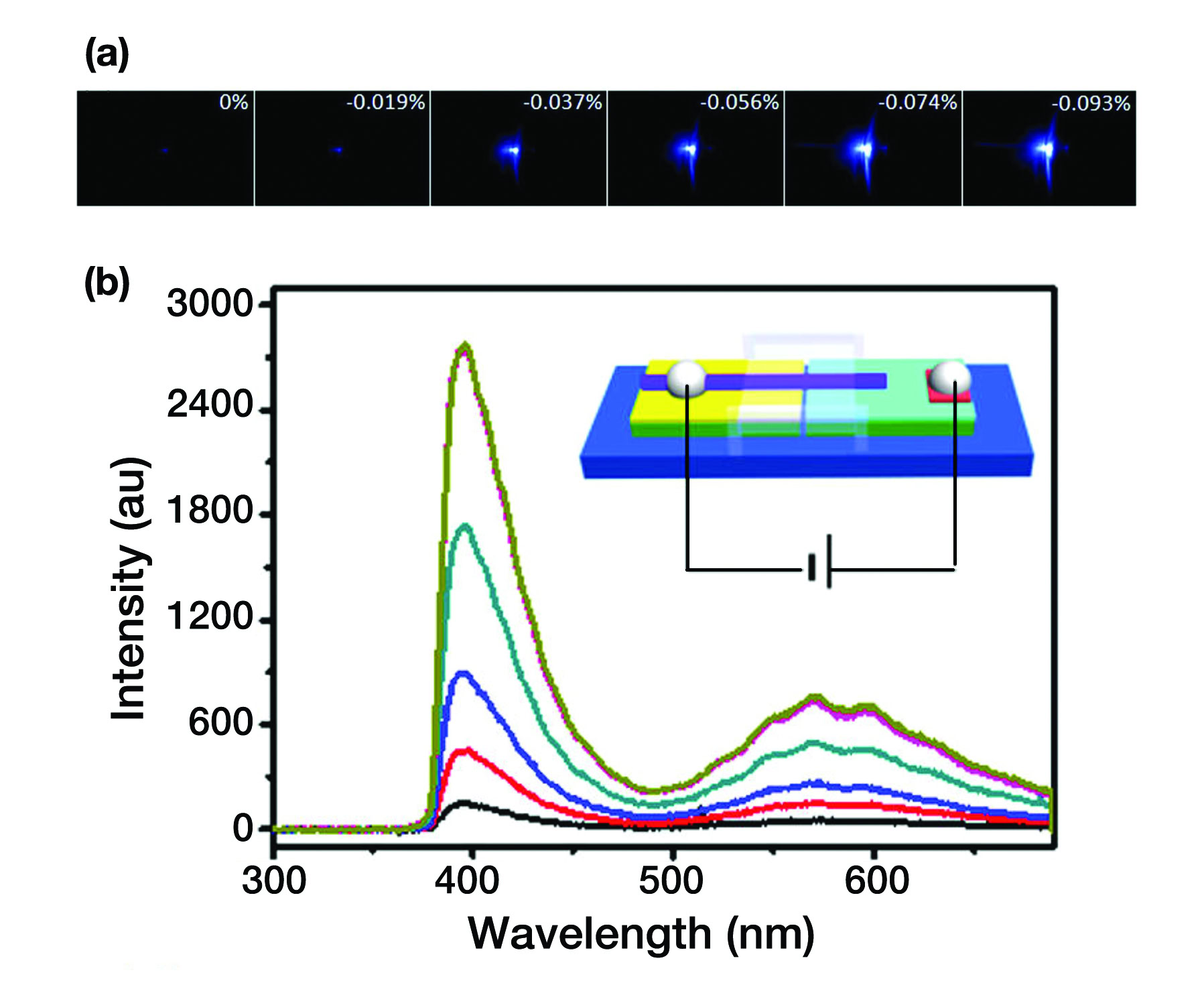
Figure 4. (a.) Optical images showing the strain-dependent emission intensity from a n-ZnO/p-GaN LED. (b) Electroluminescence spectra of the LED subject to various strains at a bias of 9 V. Adapted with permission from Reference 11. Copyright 2011, American Chemical Society. Credit: Yang et al., Nano Lett.
A similar effect also exists in PV devices, whose performance relies on effective electron–hole separation at a semiconductor heterojunction. The built-in field at the heterojunction provides a critical driving force for charge separation and, thus, dictates open-circuit voltage and short-circuit current. When a PV structure involves a piezoelectric semiconductor, the presence of Ppz may lead to a considerable change of free carrier distributions in the piezoelectric material and its adjacent semiconductor or metal contacts and, thus, influences the device performance.
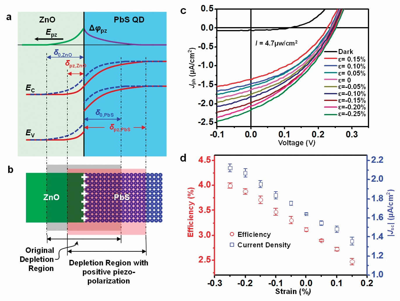
Figure 5. (a) The tailoring of the quantum dot solar cells (QDSC) band diagram when a positive Ppz appears at the ZnO–PbS interface. (b) Schematic illustration of corresponding change of the depletion regions in ZnO–PbS QD assembly. (c) J–V characteristics of a ZnO–PbS QDSC when the cell was subjected to various strains. (d) Plot of QDSC efficiency (red circles) and Jsc (blue squares) as a function of strain. Adapted from Reference 13. Credit: Shi et al., Adv. Mater.
One example has been demonstrated based on a n-ZnO–p-PbS quantum dot (QD) heterostructure, where the built-in field in the depleted PbS layer (φbi, PbS) is essential to charge extraction from the QD layer.13 Additional driving force could be expected when interfacial charge redistribution is induced by Ppz from strained ZnO. Figure 5(a) shows that, when positive Ppz appears at the ZnO–PbS interface, conduction and valence bands of PbS are bent further downward, producing a sharper, extended built-in field, which is preferable for sweeping excitons apart. In this scenario, the driving force for extracting electrons from the PbS QD assemblage is augmented to (φbi,PbS + Δφpz,PbS), and the width of the depletion region in PbS under zero external bias expands accordingly. This enlarged depletion region in the PbS QD layer is necessary for enhanced charge extraction. Meanwhile, the positive Ppz also may yield a shorter depletion region (δpz,ZnO) and shallower band bending on the ZnO side. Figure 5(b) schematically illustrates the overall change of depletion region at the ZnO–PbS interface. Therefore, positive Ppz at the ZnO–PbS interface is a favorable condition for charge extraction.
The Ppz-engineered PV performance was tested on flexible QD solar cells (QDSCs) fabricated using p-type PbS QDs and an n-type textured, (0001) orientation ZnO thin film. Appreciable change in current density (Jph) occurred under various strains (Fig. 5(c)). A linear relationship was identified from the plot of Jsc versus strain (blue squares in Fig. 5(d)), where Jsc exhibited a 0.02 μA/cm2 (or 1.1%) increase per 0.01% strain drop. Under zero strain, the efficiency of the QDSC was ~3.1% (red circles in Fig. 5(d)). Approximately 4.0% efficiency was obtained at a compressive strain of –0.25%, corresponding to a ~30% improvement. The efficiency also exhibited an approximately linear relationship with strain within the testing range (-0.25% – 0.15%), where a 1.2% efficiency enhancement per 0.01% strain drop was identified.
More significant band shifting in the piezoelectric material would be observed if the external contact material, for example, a polymer, had a very low carrier density. Depending on its electrical permittivity, the screening length of a polymer can be fairly large and the Ppz-induced electric field can be sensed far away from the interface in the polymer. This situation was first demonstrated in a polymer solar cell, where ZnO MWs served as electron conductors and poly(3-hexylthiophene) (P3HT) was the photon absorber.14 By straining the ZnO MW under photo-illumination, the cell’s open-circuit voltage increased when positive Ppz appeared at the ZnO–P3HT interface and lowered the conduction band of ZnO. A similar effect also has been observed from a ferroelectric poly(vinylidene fluoride) (PVDF)–P3HT heterostructure, where the permanent polarization from PVDF enhances the PV performance.15 So far, all the experimental evidence indicates that the piezotronic effect holds great promise for improving the performance of PV devices by enhancing the effectiveness of charge extraction and modulating the open-circuit voltage.
Piezocatalysis—Straining to split water
In addition to modulating regular semiconductor functions, coupling piezopotential with electrochemical processes creates a new effect, denoted as piezocatalysis. Because the strain state and electronic state of these materials are strongly coupled, piezocatalysis could be prominent in piezoelectric materials. Piezocatalysis is the product of an intimate interaction between the native electronic state of the piezoelectric material, the chemistry of the surrounding medium, and a strain-induced piezoelectric potential.
Mechanically deforming a piezoelectric material induces a perfuse electric field that augments the energetics of free and bound charges throughout the material. The thermodynamic feasibility and kinetics of electrochemical processes occurring at the surface of the piezoelectric material is sensitive to the electrochemical potential difference between charges on the piezoelectric’s surface and in the surrounding medium. Thus, piezoelectric potential, which can affect dramatically the difference between these electrochemical potentials, is a new means of modulating the material’s electrochemical activity via its strain state.
Recently, we demonstrated a piezocatalysis process in a strained ferroelectric Pb(Mg1/3Nb2/3)O3·32PbTiO3 (PMN-PT) beam in a deionized water system. We observed that hydrogen evolution from the water depended strongly on the material’s piezoelectric potential.16 The experiments measured hydrogen gas evolution as a function of time during mechanical oscillation of the PMN-PT cantilever in deionized water at select frequencies (Fig. 6(a)). The hydrogen concentration increased at a rate of ~0.22 ppb/s at 10 Hz oscillation. At 20 Hz oscillation, the hydrogen-gas concentration increased at a rate of ~0.68 ppb/s, demonstrating that more strain cycles could result in a higher hydrogen output per unit time.
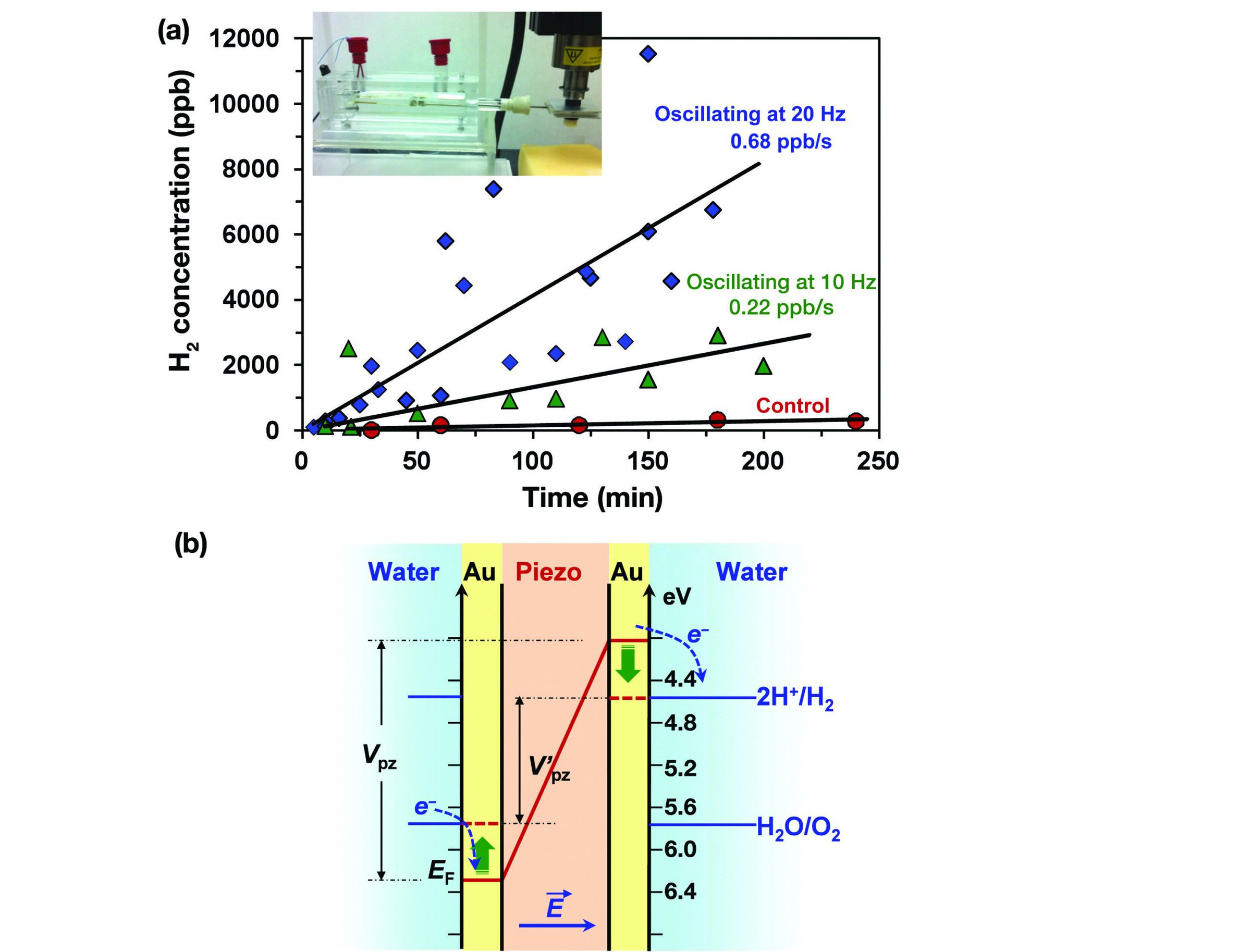
Figure 6. (a) H2 concentrations measured as a function of oscillating time of the piezoelectric beam in deionized water with a frequency of 10 Hz (triangles) and 20 Hz (diamonds). A silicon cantilever with identical configuration was used as a control (circles). Inset is a photo of the piezocatalysis system. (b) Proposed mechanism of piezocatalysis at the piezoelectric–water interface. Adapted from Reference 16.Credit: Starr et al., Angew. Chem. Int. Ed.
The electrical-to-chemical energy conversion efficiency (piezocatalytic efficiency) was estimated by comparing the total surface charge generated on the strained piezoelectric material to the amount of hydrogen-gas produced. The efficiency per oscillation was less than 0.7% even under the favorable condition of high piezoelectric potential. However, it could be improved to 2%–2.4% given sufficient time for piezocatalyzed electrochemical reactions to proceed.
The water reduction–oxidation system serves as a good example to illustrate the fundamental principle of piezocatalysis. Figure 6(b) demonstrates a means by which piezopotential is sufficient to create a favorable energetic landscape for generating Faradic currents on opposing gold electrode surfaces, promoting the reduction of protons in solution (evolving hydrogen-gas) and the oxidation of water.
In the limit where the piezoelectric material is a perfect dielectric, the appearance of piezopotential induces a linear shift of the Fermi level. Accordingly, the electron energy levels of both electrodes shift by an equal and opposite amount and the difference is the observed piezoelectric voltage output (solid red lines in Fig. 6(b)). This electronic perturbation induced by the mechanical deformation modifies the electrons’ energy in the gold electrodes and moves it away from equilibrium. The electrochemical potential differences between the electrode and solution are a driving force for electron transfer across the electrode–solution interface and thus induce electrochemical reactions. This process is similar to that which occurs in an electrolysis system, where an applied bias disrupts the Fermi-level equilibrium across the interface resulting in a driving force for electrochemical reactions. Therefore, when the potential on the negative electrode exceeds the proton reduction potential (right Au electrode in Fig. 6(b)), electrons of sufficient energy transfer from the electrode to protons on or near the surface, producing hydrogen. Similarly, when unoccupied electron energy levels of the electrode are made sufficiently positive in potential so as to exist below the water oxidation potential (left Au electrode in Fig. 6(b)), electrons transfer from water molecules to the electrode, producing oxygen.
Such piezoelectric-potential-driven electrochemical reactions create Faradic currents in the electrolyte and deplete piezoelectric-induced surface charge. Therefore, the piezoelectric potential drops accordingly, and eventually the reactions cease when the electron energy levels are no longer energetically favorable for net charge transfer (dashed red lines in Fig. 6(b)).
In addition to piezocatalyzed water splitting, numerous recent studies have confirmed the broader correlation between electrochemical activity and Ppz. For example, a study conducted using ferroelectric PVDF demonstrated that in-situ piezopotential can influence lithium-ion battery charging behavior.17 Also, electrochemical deposition can be selectively activated by the ferroelectric domain polarization.18 Thus, the novel coupling effect between Ppz and electrochemical processes emboldens a new and promising strategy for mechanically tailoring interface energetics and chemistry.
Conclusion
Piezotronics is an exciting new interdisciplinary field bridging between piezoelectrics and semiconductors. Promising proof-of-principle devices and systems are revolutionizing our understanding and practice of strain-regulated semiconductor functions. So far, the piezotronic effect has been used to
- Create local potential wells for enhanced LED quantum efficiency;
- Improve performance in GaN–InGaN quantum well lasers;
- Form electromechanical memory diodes;
- Increase open-circuit voltage and photocurrent extraction in PV and PEC devices; and
- Activate or facilitate electrochemical reactions.
Considering that Ppz depends directly upon the linear piezoelectric coefficient and the strain tensor, a more pronounced piezotronic effect can be obtained by using
- Materials that are capable of sustaining large strains without failure and
- Making use of certain piezoelectric materials that have pronounced piezoelectric coefficients and attractive semiconductor functionality.
The first case results in a more rugged piezoelectric component capable of enduring substantial strain. A design where peripheral, robust, strained piezoelectric films sandwich an active semiconductor heterojunction located within a neutral strain axis is a conceivable architecture for enhancing piezotronic performance.
A key challenge facing the second case is the low conductivity of the piezoelectric materials in conjunction with their pronounced piezoelectric coefficients. In devices whose functionality depends on the transport of charge carriers, this impediment cannot be overstated. A peripheral approach, where the piezoelectric material itself does not take part in the active heterojunction, may alleviate the problem. Alternatively, GaN and many other III–V wurtzite materials are the core semiconductor components in solar cells, lasers, LEDs, and PEC cells. These materials also exhibit appreciable piezoelectric effect, and thus make good candidates for using the piezotronic effect to regulate their functionalities.
In general, piezotronics brings new knowledge to classic semiconductor theories, where semiconductor band theory and the behaviors of electrons and holes are interpreted with additional contributions from Ppz. Piezotronics also introduces a new concept to the classic piezoelectric electromechanical coupling effect by addressing the contributions from free-charges, junction materials, surface and interface properties, and external illumination. New science obtained from the coupling between crystal structure, mechanical strain and electronic properties opens a new route toward designing, operating, and enhancing electronic, optoelectronic, photovoltaic, and even catalytic materials and systems. Piezotronics will find a significant role in the operational principles of flexible devices, MEMs, sensors, human-CMOS interfacing, and energy conversion and storage systems.
Acknowledgements
The author thanks Zhong Lin Wang at Georgia Institute of Technology for his pioneering work on piezotronics, as well as J. Shi and M. Starr for their contributions to the work in this article. The author gratefully acknowledges the financial support of DARPA under Grant No. N66001-11-1-4139 and the National Science Foundation under Grant No. CMMI-1148919.

Related Articles

Market Insights
Next-gen superconducting ceramics could change how we travel and much more
Forty years ago, two physicists from IBM’s research laboratory in Zürich, Switzerland, reported a groundbreaking discovery: Superconductivity, or the quantum mechanical phenomenon in which certain materials exhibit zero electrical resistance when cooled, could be achieved at higher temperatures using ceramics. Superconductivity had been discovered decades before, but its applications had…

Market Insights
Why most AI manufacturing projects fail and how to fix it
Artificial intelligence is reshaping advanced manufacturing, especially processes involving ceramics, glasses, and other hard or brittle materials. But adopting AI is far more difficult than simply buying software and connecting machines. Manufacturers must understand the advantages and limitations of different models, so they can determine where AI fits best within…

Bulletin Features
Radiation effects on rare earth chemistry in molten salts for nuclear applications
Across the nuclear energy sector, molten salts are shaping the next generation of nuclear technologies, from advanced power reactors to used nuclear fuel recycling. In molten salt reactors (MSRs), molten salts uniquely serve as both the primary coolant and fuel medium, a dual role that sets MSRs apart from conventional…